SNVS769J March 2000 – December 2014 LM2940-N , LM2940C
PRODUCTION DATA.
- 1 Features
- 2 Applications
- 3 Description
- 4 Revision History
- 5 Pin Configuration and Functions
- 6 Specifications
- 7 Detailed Description
- 8 Application and Implementation
- 9 Power Supply Recommendations
- 10Layout
- 11Device and Documentation Support
- 12Mechanical, Packaging, and Orderable Information
封装选项
请参考 PDF 数据表获取器件具体的封装图。
机械数据 (封装 | 引脚)
- NDE|3
- NGN|8
- DCY|4
- KTT|3
- NEB|3
散热焊盘机械数据 (封装 | 引脚)
订购信息
8 Application and Implementation
NOTE
Information in the following applications sections is not part of the TI component specification, and TI does not warrant its accuracy or completeness. TI’s customers are responsible for determining suitability of components for their purposes. Customers should validate and test their design implementation to confirm system functionality.
8.1 Application Information
The LM2940-N and LM2940C positive voltage regulators feature the ability to source 1 A of output current with a dropout voltage of typically 0.5 V and a maximum of 1 V over the entire temperature range. The output capacitor, COUT, must have a capacitance value of at least 22 µF with an ESR of at least 100 mΩ, but no more than 1 Ω. The minimum capacitance value and the ESR requirements apply across the entire expected operating ambient temperature range.
8.2 Typical Application
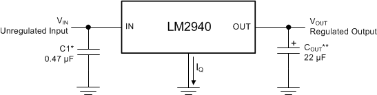
**COUT must be at least 22 μF to maintain stability. May be increased without bound to maintain regulation during transients. Locate as close as possible to the regulator. This capacitor must be rated over the same operating temperature range as the regulator and the ESR is critical; see curve.
8.2.1 Design Requirements
Table 1. Design Parameters
| DESIGN PARAMETER | EXAMPLE VALUE |
|---|---|
| Input voltage range | 6 V to 26 V |
| Output voltage range | 8 V |
| Output current range | 5 mA to 1 A |
| Input capacitor value | 0.47 µF |
| Output capacitor value | 22 µF minimum |
| Output capacitor ESR range | 100 mΩ to 1 Ω |
8.2.2 Detailed Design Procedure
8.2.2.1 External Capacitors
The output capacitor is critical to maintaining regulator stability, and must meet the required conditions for both equivalent series resistance (ESR) and minimum amount of capacitance.
8.2.2.1.1 Minimum Capacitance
The minimum output capacitance required to maintain stability is 22 μF (this value may be increased without limit). Larger values of output capacitance will give improved transient response.
8.2.2.1.2 ESR Limits
The ESR of the output capacitor will cause loop instability if it is too high or too low. The acceptable range of ESR plotted versus load current is shown in the graph below. It is essential that the output capacitor meet these requirements, or oscillations can result.
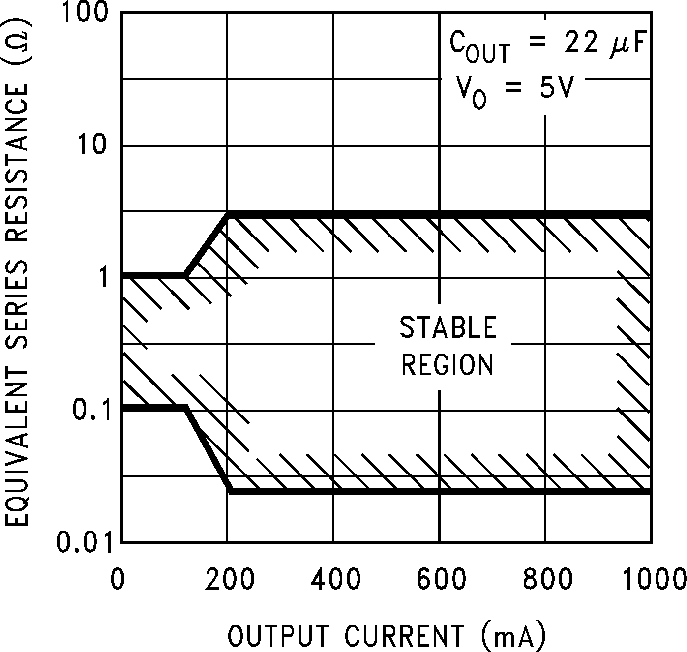 Figure 27. Output Capacitor ESR Limits
It is important to note that for most capacitors, ESR is specified only at room temperature. However, the designer must ensure that the ESR will stay inside the limits shown over the entire operating temperature range for the design.
For aluminum electrolytic capacitors, ESR will increase by about 30X as the temperature is reduced from 25°C to −40°C. This type of capacitor is not well-suited for low temperature operation.
Solid tantalum capacitors have a more stable ESR over temperature, but are more expensive than aluminum electrolytics. A cost-effective approach sometimes used is to parallel an aluminum electrolytic with a solid tantalum, with the total capacitance split about 75/25% with the aluminum being the larger value.
If two capacitors are paralleled, the effective ESR is the parallel of the two individual values. The flatter ESR of the tantalum will keep the effective ESR from rising as quickly at low temperatures.
8.2.3 Application Curves
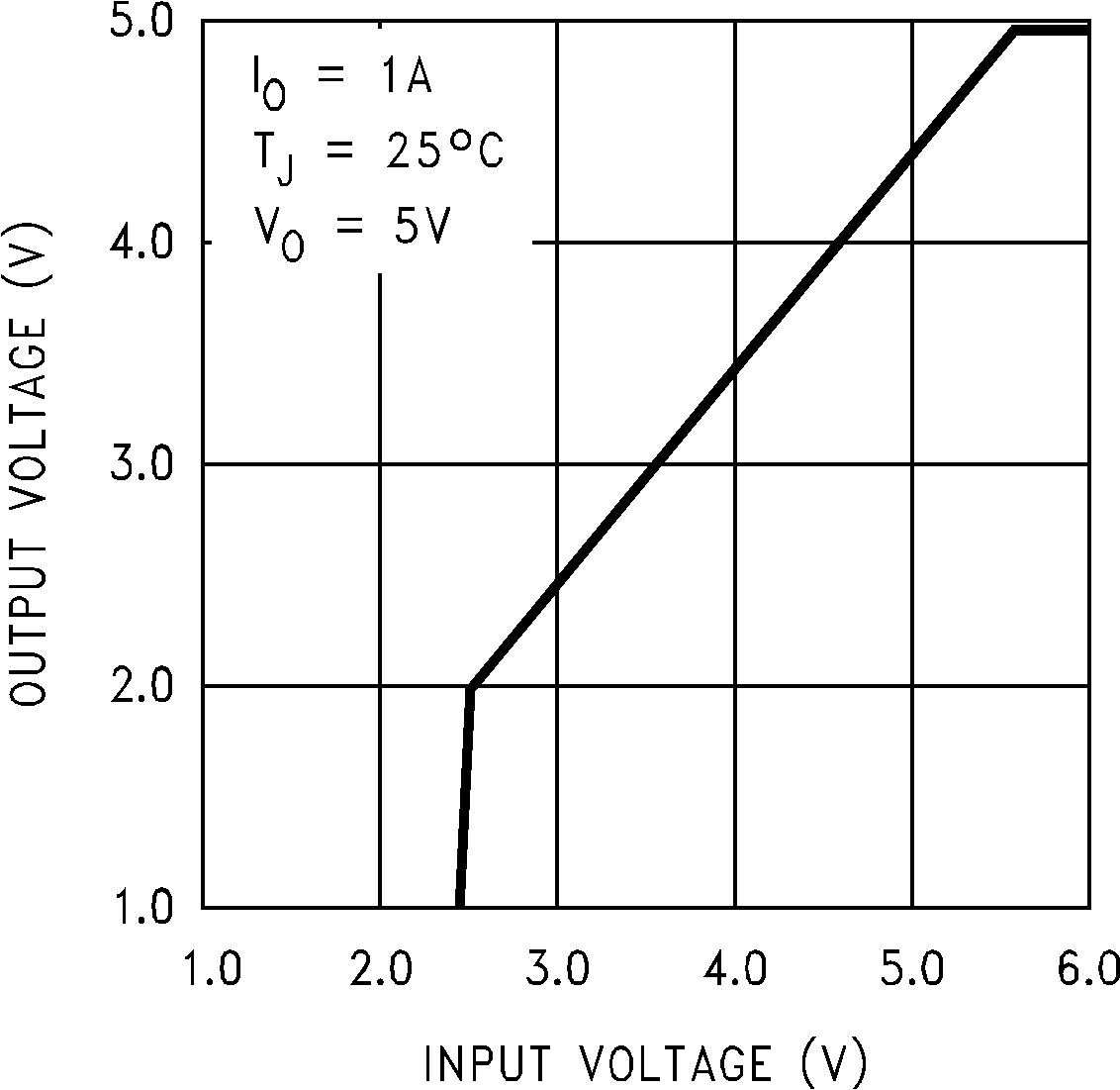 Figure 28. Low Voltage Behavior
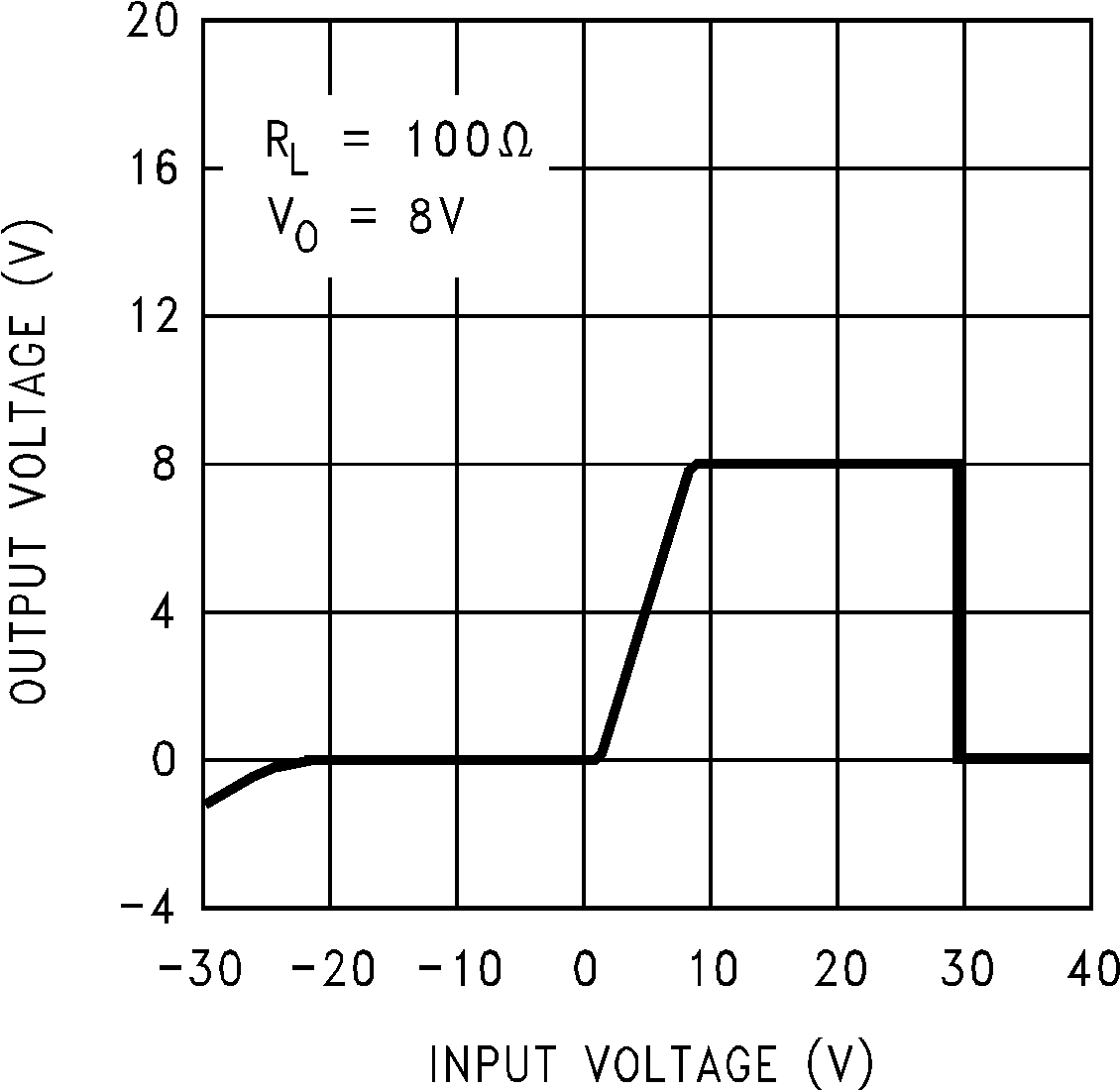 Figure 29. Output at Voltage Extremes