ZHCSNF0B May 2018 – October 2021 ISOW1412 , ISOW1432
PRODMIX
- 1 特性
- 2 应用
- 3 说明
- 4 Revision History
- 5 说明(续)
- 6 Device Comparison Table
- 7 Pin Configuration and Functions
-
8 Specifications
- 8.1 Absolute Maximum Ratings
- 8.2 Recommended Operating Conditions
- 8.3 Thermal Information
- 8.4 Power Ratings
- 8.5 Insulation Specifications
- 8.6 Safety-Related Certifications
- 8.7 Safety Limiting Values
- 8.8 Electrical Characteristics
- 8.9 Supply Current Characteristics at VISOOUT = 3.3 V
- 8.10 Supply Current Characteristics at VISOOUT = 5 V
- 8.11 Switching Characteristics at VISOOUT = 3.3 V
- 8.12 Switching Characteristics at VISOOUT = 5 V
- 8.13 Insulation Characteristics Curves
- 8.14 Typical Characteristics
- 9 Parameter Measurement Information
- 10Detailed Description
- 11Application and Implementation
- 12Power Supply Recommendations
- 13Layout
- 14Device and Documentation Support
- 15Mechanical, Packaging, and Orderable Information
9 Parameter Measurement Information
In this section, GND1 = GNDIO, GND2 = GISOIN
unless otherwise noted.
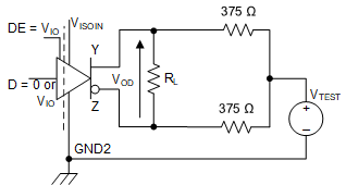 Figure 9-1 Driver
Voltages


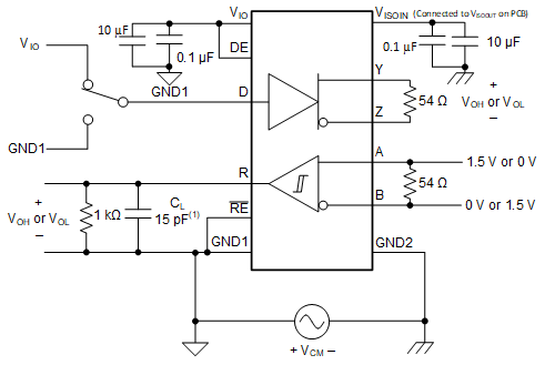

 Figure 9-6 Driver
Enable and Disable Times

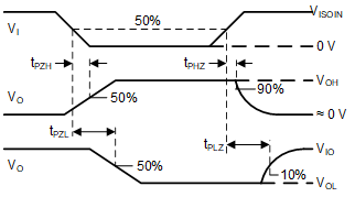 Figure 9-8 Receiver
Enable and Disable Times
 Figure 9-9 Receiver
Enable and Disable Times


 Figure 9-1 Driver
Voltages
RL = 100 Ω for RS-422,
RL = 54 Ω for RS-485
Figure 9-2 Driver
Voltages
CL includes fixture
and instrumentation capacitance
Figure 9-3 Driver
Switching Specifications
Includes probe and fixture
capacitance
Pass-fail criteria: Device is tested in both half-duplex and full-duplex
conditions. Both the signal path and power path should be in specification
compliant region during the application of CMTI pulse. This means no bit flips
on R, and both VISOOUT and Driver VOD should be within
specifications mentioned in electrical characterisitcs table.
Figure 9-4 Common
Mode Transient Immunity (CMTI)—Full Duplex
CL includes fixture
and instrumentation capacitance
Figure 9-5 Driver
Enable and Disable Times Figure 9-6 Driver
Enable and Disable Times
CL includes fixture
and instrumentation capacitance
Figure 9-7 Receiver
Switching Specifications Figure 9-8 Receiver
Enable and Disable Times
 Figure 9-9 Receiver
Enable and Disable Times
The driver should not sustain any
damage with this configuration
Figure 9-10 Short-Circuit Current
Limiting
The input pulse
is supplied by a generator having the following characteristics: PRR ≤ 50 kHz,
50% duty cycle, tr ≤ 3 ns, tf ≤ 3 ns, ZO = 50
Ω. At the input, 50-Ω resistor is required to terminate the input generator
signal. The resistor is not required in the actual application. CL =
15 pF and includes instrumentation and fixture capacitance within ±20%.
Figure 9-11 GPIO Channel: Switching
Characteristics Test Circuit and Voltage Waveforms