ZHCSID5E April 2018 – September 2019 ISO1410 , ISO1412 , ISO1430 , ISO1432 , ISO1450 , ISO1452
UNLESS OTHERWISE NOTED, this document contains PRODUCTION DATA.
- 1 特性
- 2 应用
- 3 说明
- 4 修订历史记录
- 5 说明 (续)
- 6 Device Options
- 7 Pin Configuration and Functions
-
8 Specifications
- 8.1 Absolute Maximum Ratings
- 8.2 ESD Ratings
- 8.3 Recommended Operating Conditions
- 8.4 Thermal Information
- 8.5 Power Ratings
- 8.6 Insulation Specifications
- 8.7 Safety-Related Certifications
- 8.8 Safety Limiting Values
- 8.9 Electrical Characteristics: Driver
- 8.10 Electrical Characteristics: Receiver
- 8.11 Supply Current Characteristics: Side 1 (ICC1)
- 8.12 Supply Current Characteristics: Side 2 (ICC2)
- 8.13 Switching Characteristics: Driver
- 8.14 Switching Characteristics: Receiver
- 8.15 Insulation Characteristics Curves
- 8.16 Typical Characteristics
- 9 Parameter Measurement Information
- 10Detailed Description
- 11Application and Implementation
- 12Power Supply Recommendations
- 13Layout
- 14器件和文档支持
- 15机械、封装和可订购信息
封装选项
请参考 PDF 数据表获取器件具体的封装图。
机械数据 (封装 | 引脚)
- DW|16
散热焊盘机械数据 (封装 | 引脚)
- DW|16
订购信息
7 Pin Configuration and Functions
DW Package
16-Pin SOIC
Full-Duplex Device Top View

Pin Functions: Full-Duplex Device
| PIN | I/O | DESCRIPTION | |
|---|---|---|---|
| NAME | NO. | ||
| A | 14 | I | Receiver non-inverting input on the bus side |
| B | 13 | I | Receiver inverting input on the bus side |
| D | 6 | I | Driver input |
| DE | 5 | I | Driver enable. This pin enables the driver output when high and disables the driver output when low or open. |
| GND1(1) | 2 | — | Ground connection for VCC1 |
| GND1(1) | 8 | — | Ground connection for VCC1 |
| GND2(1) | 9 | — | Ground connection for VCC2 |
| GND2(1) | 15 | — | Ground connection for VCC2 |
| NC(2) | 7 | — | No internal connection |
| NC(2) | 10 | — | No internal connection |
| R | 3 | O | Receiver output |
| RE | 4 | I | Receiver enable. This pin disables the receiver output when high or open and enables the receiver output when low. |
| VCC1 | 1 | — | Logic-side power supply |
| VCC2 | 16 | — | Transceiver-side power supply |
| Y | 11 | O | Driver non-inverting output |
| Z | 12 | O | Driver inverting output |
(1) For Logic side, both Pin 2 and Pin 8 must be connected to GND1. For Bus side, both Pin 9 and Pin 15 must be connected to GND2.
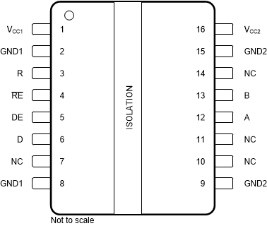
DW Package
16-Pin SOIC
Half-Duplex Device Top View

Pin Functions: Half-Duplex Device
| PIN | I/O | DESCRIPTION | |
|---|---|---|---|
| NAME | NO. | ||
| A | 12 | I/O | Transceiver non-inverting input or output (I/O) on the bus side |
| B | 13 | I/O | Transceiver inverting input or output (I/O) on the bus side |
| D | 6 | I | Driver input |
| DE | 5 | I | Driver enable. This pin enables the driver output when high and disables the driver output when low or open. |
| GND1(1) | 2 | — | Ground connection for VCC1 |
| GND1(1) | 8 | — | Ground connection for VCC1 |
| GND2(1) | 9 | — | Ground connection for VCC2 |
| GND2(1) | 15 | — | Ground connection for VCC2 |
| NC(2) | 7 | — | No internal connection |
| NC(2) | 10 | — | No internal connection |
| NC(2) | 11 | — | No internal connection |
| NC(2) | 14 | — | No internal connection |
| R | 3 | O | Receiver output |
| RE | 4 | I | Receiver enable. This pin disables the receiver output when high or open and enables the receiver output when low. |
| VCC1 | 1 | — | Logic-side power supply |
| VCC2 | 16 | — | Transceiver-side power supply |
(1) For Logic side, both Pin 2 and Pin 8 must be connected to GND1. For Bus side, both Pin 9 and Pin 15 must be connected to GND2.
(2) Device functionality is not affected if NC pins are connected to supply or ground on PCB