ZHCSJJ1A March 2019 – May 2021 INA302-Q1 , INA303-Q1
PRODUCTION DATA
- 1 特性
- 2 应用
- 3 说明
- 4 Revision History
- 5 Pin Configuration and Functions
- 6 Specifications
- 7 Detailed Description
- 8 Application and Implementation
- 9 Power Supply Recommendations
- 10Layout
- 11Device and Documentation Support
- 12Mechanical, Packaging, and Orderable Information
8.1.2 Input Filtering
The integrated comparators in the INA30x-Q1 are very accurate at detecting out-of-range events because of the low offset voltage; however, noise present at the input of the current-sense amplifier and noise internal to the device can make the offset appear larger than specified. The most obvious effect that external noise can have on the operation of a comparator is to cause a false alert condition. If a comparator detects a large noise transient coupled into the signal, the device can easily falsely interpret this transient as an overrange condition.
External filtering helps reduce the amount of noise that reaches the comparator and reduce the likelihood of a false alert from occurring because of external noise. The trade-off to adding this noise filter is that the alert response time is increased because the input signal and the noise are filtered. Figure 8-1 shows the implementation of an input filter for the device.
 Figure 8-1 Input Filter Implementation
Limiting the amount of input resistance used in this filter is important because this resistance can have a significant effect on the input signal that reaches the device input pins by adversely affecting the gain error of the device. A typical system implementation involves placing the current-sensing resistor very near the device so the traces are very short and the trace impedance is very small. This layout helps reduce coupling of additional noise into the measurement. Under these conditions, the characteristics of the input bias currents have minimal effect on device performance.
As shown in Figure 8-2, the input bias currents increase in opposite directions when the differential input voltage increases. This increase results from the design of the device that allows common-mode input voltages to far exceed the device supply voltage range. When input filter resistors are placed in series with the unequal input bias currents, unequal voltage drops are developed across the input resistors. The difference between these two drops appears as an added signal that (in this case) subtracts from the voltage developed across the current-sensing resistor, thus reducing the signal that reaches the device input pins. Smaller-value input resistors reduce this effect of signal attenuation to allow for a more accurate measurement.
 Figure 8-2 Input Bias Current vs Differential Input Voltage
The internal bias network present at the input pins shown in Figure 8-3 is responsible for the mismatch in input bias currents that is shown in Figure 8-2. If additional external series filter resistors are added to the circuit, the mismatch in bias currents results in a mismatch of voltage drops across the filter resistors. This mismatch creates a differential error voltage that subtracts from the voltage developed at the shunt resistor. This error results in a voltage at the device input pins that is different than the voltage developed across the shunt resistor. Without the additional series resistance, the mismatch in input bias currents has little effect on device operation. The amount of error these external filter resistors add to the measurement is calculated using Equation 6, where the gain error factor is calculated using Equation 5.

The amount of variance in the differential voltage present at the device input relative to the voltage developed at the shunt resistor is based both on the external series resistance value as well as the internal input resistors, R3 and R4 (or RINT as illustrated in Figure 8-3). The reduction of the shunt voltage reaching the device input pins appears as a gain error when comparing the output voltage relative to the voltage across the shunt resistor. A factor can be calculated to determine the amount of gain error that is introduced by the addition of external series resistance. The equation used to calculate the expected deviation from the shunt voltage to what is measured at the device input pins is given in Equation 5:
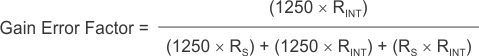
where
- RINT is the internal input resistor (R3 and R4).
- RS is the external series resistance.
With the adjustment factor from Equation 5, including the device internal input resistance, this factor varies with each gain version, as shown in Table 8-2. Each individual device gain error factor is shown in Table 8-3.
| PRODUCT | GAIN | RINT (kΩ) |
|---|---|---|
| INA30xA1-Q1 | 20 | 12.5 |
| INA30xA2-Q1 | 50 | 5 |
| INA30xA3-Q1 | 100 | 2.5 |
| PRODUCT | SIMPLIFIED GAIN ERROR FACTOR |
|---|---|
| INA30xA1-Q1 | 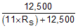 |
| INA30xA2-Q1 |  |
| INA30xA3-Q1 |  |
The gain error that is expected from the addition of the external series resistors is then calculated based on Equation 6:

For example, using an INA302A2-Q1 and the corresponding gain error equation from Table 8-3, a series resistance of 10 Ω results in a gain error factor of 0.99. The corresponding gain error is then calculated using Equation 6, resulting in a gain error of approximately 1% solely because of the external 10-Ω series resistors.