SNLS316G September 2009 – December 2015 DS90UR907Q-Q1
PRODUCTION DATA.
- 1 Features
- 2 Applications
- 3 Description
- 4 Revision History
- 5 Pin Configuration and Functions
-
6 Specifications
- 6.1 Absolute Maximum Ratings
- 6.2 ESD Ratings—JEDEC
- 6.3 ESD Ratings—IEC and ISO
- 6.4 Recommended Operating Conditions
- 6.5 Thermal Information
- 6.6 DC Electrical Characteristics
- 6.7 Recommended Timing for the Serial Control Bus
- 6.8 Switching Characteristics
- 6.9 DC and AC Serial Control Bus Characteristics
- 6.10 Typical Characteristics
-
7 Detailed Description
- 7.1 Overview
- 7.2 Functional Block Diagram
- 7.3 Feature Description
- 7.4 Device Functional Modes
- 7.5 Programming
- 8 Application and Implementation
- 9 Power Supply Recommendations
- 10Layout
- 11Device and Documentation Support
- 12Mechanical, Packaging, and Orderable Information
1 Features
- 5-MHz to 65-MHz Support (140-Mbps to 1.82-Gbps Serial Link)
- 5-Channel (4 data + 1 clock) FPD-Link Receiver Inputs
- AC-Coupled STP Interconnect up to 10 Meters in Length
- Integrated Output Termination
- At Speed Link BIST Mode
- Optional I2C Compatible Serial Control Bus
- RGB888 + VS, HS, DE support
- Power-Down Mode Minimizes Power Dissipation
- Randomizer/Scrambler – DC-Balanced Data Stream
- Low EMI FPD-Link Input
- Selectable Output VOD and Adjustable De-Emphasis
- 1.8-V or 3.3-V Compatible Control Bus Interface
- Automotive Grade Product: AEC-Q100 Grade 2 Qualified
- >8-kV HBM and ISO 10605 ESD Rating
- Backward Compatible Mode for Operation With Older Generation Devices
2 Applications
- Automotive Display for Navigation
- Automotive Display for Entertainment
3 Description
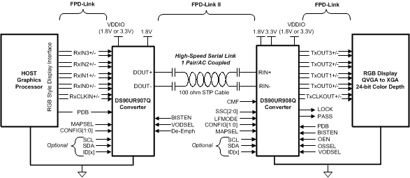
The DS90UR907Q-Q1 converts FPD-Link to FPD-Link II. It translates four LVDS data/control streams and one LVDS clock pair (FPD-Link) into a high-speed serialized interface (FPD-Link II) over a single pair. This serial bus scheme greatly eases system design by eliminating skew problems between clock and data, reduces the number of connector pins, reduces the interconnect size, weight, and cost, and overall eases PCB layout. In addition, internal DC balanced encoding is used to support AC-coupled interconnects.
The DS90UR907Q-Q1 converts, balances and level shifts four LVDS data/control streams, and embeds one LVDS clock pair (FPD-Link) to a serial stream (FPD-Link II). Up to 24 bits of RGB in the FPD-Link are serialized along with the three video control signals.
Serial transmission is optimized by a user selectable de-emphasis and differential output level select features. EMI is minimized by the use of low voltage differential signaling and spread spectrum clocking compatibility.
With fewer wires to the physical interface of the host, FPD-Link input with LVDS technology is ideal for high speed, low power and low EMI data transfer.
The device is offered in a 36-pin WQFN package and is specified over the automotive AEC-Q100 Grade 2 temperature range of –40˚C to 105˚C.
Device Information(1)
| PART NUMBER | PACKAGE | BODY SIZE (NOM) |
|---|---|---|
| DS90UR907Q-Q1 | WQFN (36) | 6.00 mm × 6.00 mm |
- For all available packages, see the orderable addendum at the end of the data sheet.
Applications Diagram
