SNLS231O September 2006 – April 2015 DS90UR124-Q1 , DS90UR241-Q1
PRODUCTION DATA.
- 1 Features
- 2 Applications
- 3 Description
- 4 Revision History
- 5 Description (continued)
- 6 Pin Configuration and Functions
- 7 Specifications
-
8 Detailed Description
- 8.1 Overview
- 8.2 Functional Block Diagram
- 8.3 Feature Description
- 8.4 Device Functional Modes
- 9 Application and Implementation
- 10Power Supply Recommendations
- 11Layout
- 12Device and Documentation Support
- 13Mechanical, Packaging, and Orderable Information
9 Application and Implementation
NOTE
Information in the following applications sections is not part of the TI component specification, and TI does not warrant its accuracy or completeness. TI’s customers are responsible for determining suitability of components for their purposes. Customers should validate and test their design implementation to confirm system functionality.
9.1 Application Information
9.1.1 Using the DS90UR241 and DS90UR124
The DS90UR241/DS90UR124 Serializer/Deserializer (SERDES) pair sends 24 bits of parallel LVCMOS data over a serial LVDS link up to 1.03 Gbps. Serialization of the input data is accomplished using an onboard PLL at the Serializer which embeds clock with the data. The Deserializer extracts the clock/control information from the incoming data stream and deserializes the data. The Deserializer monitors the incoming clock information to determine lock status and will indicate lock by asserting the LOCK output high.
9.1.2 Display Application
The DS90URxxx-Q1 chipset is intended for interface between a host (graphics processor) and a Display. It supports an 18-bit color depth (RGB666) and up to 1280 × 480 display formats. In a RGB666 configuration 18 color bits (R[5:0], G[5:0], B[5:0]), Pixel Clock (PCLK) and 3 control bits (VS, HS and DE) along with 3 spare bits are supported across the serial link with PCLK rates from 5 to 43 MHz.
9.1.3 Typical Application Connection
Figure 22 shows a typical application of the DS90UR241 Serializer (SER). The LVDS outputs use a 100-Ω termination and 100-nF coupling capacitors to the line. Bypass capacitors are placed near the power supply pins. At a minimum, three 0.1-uF capacitors should be used for local bypassing. A system GPO (General Purpose Output) controls the TPWDNB pin. In this application the TRFB pin is tied High to latch data on the rising edge of the TCLK. The DEN signal is not used and is tied High also. The application is to the companion Deserializer (DS90UR124) so the RAOFF pin is tied low to scramble the data and improve link signal quality. In this application the link is typical, therefore the VODSEL pin is tied Low for the standard LVDS swing. The pre-emphasis input uses a resistor to ground to set the amount of pre-emphasis desired by the application.
Figure 26 shows a typical application of the DS90UR124 Deserializer (DES). The LVDS inputs use a 100-Ω termination and 100-nF coupling capacitors to the line. Bypass capacitors are placed near the power supply pins. At a minimum, four 0.1-uF capacitors should be used for local bypassing. A system GPO (general-purpose output) controls the RPWDNB pin. In this application the RRFB pin is tied High to strobe the data on the rising edge of the RCLK. The REN signal is not used and is tied High also. The application is to the companion Serializer (DS90UR241) so the RAOFF pin is tied low to descramble the data. Output (LVCMOS) signal quality is set by the SLEW pin, and the PTOSEL pin can be used to reduce simultaneous output switching by introducing a small amount of delay between output banks.
9.2 Typical Applications
9.2.1 DS90UR241-Q1 Typical Application Connection
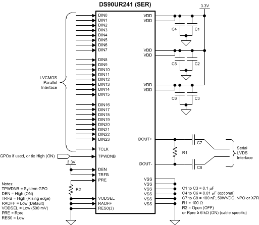 Figure 22. DS90UR241 Connection Diagram
9.2.1.1 Design Requirements
Table 3. DS90UR241 Design Parameter
| DESIGN PARAMETER | EXAMPLE VALUE |
|---|---|
| VDD | 3.3 V |
| AC Coupling Capacitor for DOUT± | 100 nF |
| DOUT± External Termination | 100 Ω |
| PCLK Frequency | 33 MHz |
9.2.1.2 Detailed Design Procedure
Figure 22 shows a typical application of the DS90UR241 serializer for an 33-MHz 18-bit Color Display Application. The DOUT± outputs must have a series external 0.1-μF AC-coupling capacitor and 100-Ω parallel termination on the high-speed serial lines. The serializer does not have an internal termination. Bypass capacitors are placed near the power supply pins. At a minimum, three 0.1-μF capacitors should be used for local device bypassing. Additional capacitors may be needed as the number and values of the capacitors will depend on meeting the power noise specification of the part. Ferrite beads may be needed on the VDDs for effective noise suppression. The interface to the graphics source is with 3.3-V LVCMOS levels. An RC delay is placed on the PDB signal to delay the enabling of the device until power is stable.
9.2.1.2.1 Power Considerations
An all LVCMOS design of the Serializer and Deserializer makes them inherently low-power devices. Additionally, the constant current source nature of the LVDS outputs minimizes the slope of the speed vs. IDD curve of LVCMOS designs.
9.2.1.2.2 Noise Margin
The Deserializer noise margin is the amount of input jitter (phase noise) that the Deserializer can tolerate and still reliably recover data. Various environmental and systematic factors include:
- Serializer: VDD noise, TCLK jitter (noise bandwidth and out-of-band noise)
- Media: ISI, VCM noise
- Deserializer: VDD noise
For a graphical representation of noise margin, see Figure 19.
9.2.1.2.3 Transmission Media
The Serializer and Deserializer are to be used in point-to-point configuration, through a PCB trace, or through twisted pair cable. In a point-to-point configuration, the transmission media needs be terminated at both ends of the transmitter and receiver pair. Interconnect for LVDS typically has a differential impedance of 100 Ω. Use cables and connectors that have matched differential impedance to minimize impedance discontinuities. In most applications that involve cables, the transmission distance will be determined on data rates involved, acceptable bit error rate and transmission medium.
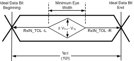
The resulting signal quality at the receiving end of the transmission media may be assessed by monitoring the differential eye opening of the serial data stream. The Receiver Input Tolerance and Differential Threshold Voltage specifications define the acceptable data eye opening. A differential probe should be used to measure across the termination resistor at the DS90UR124 inputs. Figure 23 illustrates the eye opening and relationship to the Receiver Input Tolerance and Differential Threshold Voltage specifications.
9.2.1.2.4 Live Link Insertion
The Serializer and Deserializer devices support live pluggable applications. The automatic receiver lock to random data “plug and go” hot insertion capability allows the DS90UR124 to attain lock to the active data stream during a live insertion event.
9.2.1.3 Application Curves
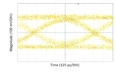 Figure 24. DS90UR241 DOUT± at 1.2 Gbps Measured at RIN± Termination; VODSEL=LOW
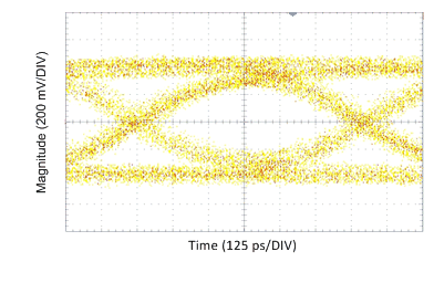 Figure 25. DS90UR241 DOUT± at 1.2 Gbps Measured at RIN± Termination; VODSEL=HIGH
9.2.2 DS90UR124 Typical Application Connection
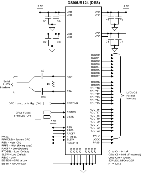 Figure 26. DS90UR124 Connection Diagram
9.2.2.1 Design Requirements
Table 4. DS90UR124 Design Parameters
| DESIGN PARAMETER | EXAMPLE VALUE |
|---|---|
| VDD | 3.3 V |
| DS90UR124-Q1 AC-Coupling Capacitor for RIN± | 100 nF |
| DS90UR124-Q1 Termination for RIN± | 100 Ω |
9.2.2.2 Detailed Design Procedure
Figure 26 shows a typical application of the DS90UR124 deserializer for an 33-MHz 18-bit Color Display Application. The RIN± inputs must have an external series 0.1-μF AC-coupling capacitor and 100-Ω parallel termination on the high-speed serial lines. The deserializer does not have an internal termination. Bypass capacitors are placed near the power supply pins. At a minimum, four 0.1-μF capacitors should be used for local device bypassing. Ferrite beads may be needed on the VDDs for effective noise suppression. Additional capacitors may be needed as the number and values of the capacitors will depend on meeting the power noise specification of the part. The interface to the display is with 3.3-V LVCMOS levels. An RC delay is placed on the PDB signal to delay the enabling of the device until power is stable.
9.2.2.3 Application Curves
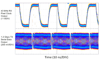 Figure 27. DS90UR241 Serial Stream and DS90UR124
43-MHz PCLK Output
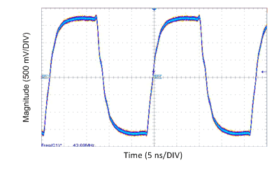 Figure 28. DS90UR124 PCLK Output at 43 MHz (Enlarged)
