ZHCSC39B February 2014 – November 2017 DRV8308
PRODUCTION DATA.
- 1 特性
- 2 应用
- 3 说明
- 4 修订历史记录
- 5 Pin Configurations and Functions
- 6 Specifications
-
7 Detailed Description
- 7.1 Overview
- 7.2 Functional Block Diagram
- 7.3
Feature Description
- 7.3.1 Hall Comparators
- 7.3.2 FG Amplifier, Comparator, and FG Output
- 7.3.3 Enable, Reset, and Clock Generation
- 7.3.4 Commutation
- 7.3.5 Commutation Logic Block Diagram
- 7.3.6 Commutation Parameters
- 7.3.7 Braking
- 7.3.8 Output Pre-Drivers
- 7.3.9 Current Limit
- 7.3.10 Charge Pump
- 7.3.11 5-V Linear Regulator
- 7.3.12 Power Switch
- 7.3.13 Protection Circuits
- 7.4 Device Functional Modes
- 7.5 Programming
- 7.6 Register Map
- 8 Application and Implementation
- 9 Power Supply Recommendations
- 10Layout
- 11器件和文档支持
- 12机械、封装和可订购信息
7 Detailed Description
7.1 Overview
The DRV8308 device controls 3-phase brushless DC motors using a speed and direction input interface and Hall signals from the motor. The device drives N-channel MOSFETs with 10-V VGS, and a configurable gate drive current of 10 to 130 mA.
There are three modes of speed input: clock frequency, clock duty cycle (pulse-width modulation), and an internal register that specifies duty cycle. In the Clock Frequency Mode, the device’s digital speed control system matches motor speed with the input clock’s frequency. Motor speed is either determined from the Halls sensors or signal on the FG input, which can be generated from a board trace underneath the motor that senses magnetic reluctance. The speed control system offers digital tuning of pole and zero frequencies and integrator gain. When properly tuned, the DRV8308 can drive motors with < 0.1% cycle jitter and fast torque compensation for varying loads. The duty cycle speed modes operate in open-loop without speed control.
When the DRV8308 device powers up, the configuration registers are set from either the one-time programmable (OTP) non-volatile memory, or from an external EEPROM (depending on the SMODE pin). After power-up, registers can be set in realtime over SPI, and the OTP memory can be permanently written once.
When the DRV8308 device begins spinning a motor, it initially uses all three Hall sensor phases to commutate. After a constant speed is reached, the LOCKn pin is pulled low and only one Hall sensor becomes used; this feature reduces jitter by eliminating the error caused by non-ideal Hall device placement and matching. Also at this time, commutation transitions to sine wave current drive (if enabled), which minimizes acoustic noise and torque ripple. Commutation timing can be tuned using the ADVANCE register for optimal performance and power efficiency.
Numerous protection circuits prevent system components from being damaged during adverse conditions. Monitored aspects include motor voltage and current, gate drive voltage and current, and device temperature . When a fault occurs, the DRV8308 device stops driving and pulls FAULTn low, in order to prevent FET damage and motor overheating.
The DRV8308 device is packaged in a compact 6 × 6-mm, 40-pin QFN with a 0.5-mm pin pitch, and operates through an industrial ambient temperature range of –40°C to 85°C.
7.2 Functional Block Diagram
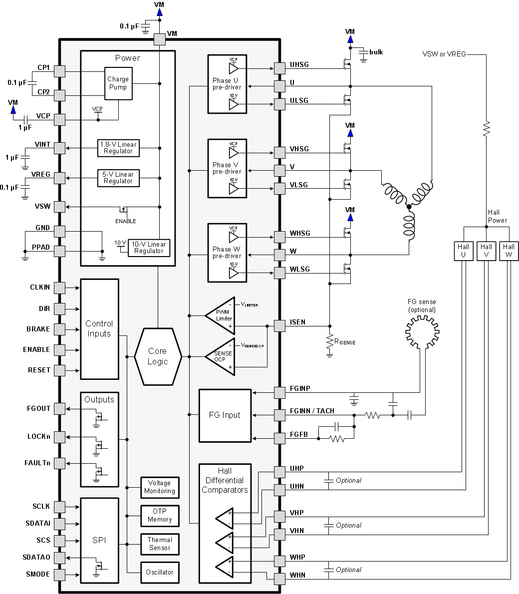
7.3 Feature Description
7.3.1 Hall Comparators
Three comparators are provided to process the raw signals from Hall effect transducers to commutate the motor. The Hall amplifiers sense zero crossings of the differential inputs and pass the information to digital logic.
The Hall amplifiers have hysteresis, and their detect threshold is centered at 0. Note, hysteresis is defined as shown in Figure 4:
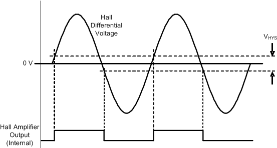 Figure 4. Hall Amplifier Hysteresis
In addition to the hysteresis, the Hall inputs are deglitched with a circuit that ignores any extra Hall transitions for a period of 20 μs after sensing a valid transition. This prevents PWM noise from being coupled into the Hall inputs, which can result in erroneous commutation.
If excessive noise is still coupled into the Hall comparator inputs, it may be necessary to add capacitors between the + and – inputs of the Hall comparators, and (or) between the input or inputs and ground.
The ESD protection circuitry on the Hall inputs implements a diode to VREG. Because of this diode, the voltage on the Hall inputs should not exceed the VREG voltage.
Since VREG is disabled in standby mode (ENABLE inactive), the Hall inputs should not be driven by external voltages in standby mode. If the Hall sensors are powered from VREG or from VSW, this is specified by the DRV8308 device; however, if the Hall sensors are powered externally, they should be disabled if the DRV8308 is put into standby mode. In addition, they should be powered-up before enabling the motor, or an invalid Hall state may cause a delay in motor operation.
7.3.2 FG Amplifier, Comparator, and FG Output
An FG amplifier and comparator provide rotational feedback from an external magnetic reluctance sensor. A diagram of the FG circuit is shown in Figure 5:
 Figure 5. FG Circuit Diagram
The output of the FG amplifier is provided on a pin, so the gain of the FG amplifier can be set by the user. Filter circuits can also be implemented.
Note that the FG signal is also fed back internally to the speed control circuits.
The FG signal that the DRV8308 device uses can be generated from a PCB trace under a motor, or it can be input from a logic-level TACH input, or it can be synthesized from the Hall sensor transitions (selectable by register FGSEL). If generated from Hall transitions, the resulting output can be either an exclusive-or function of the three Hall sensors, or the same as the HALL_U input, as shown in Figure 6.
Selection of FG operating mode is through the FGSEL register bits.
The FGOUT pin is an open-drain output and requires an external pullup resistor to the logic supply.
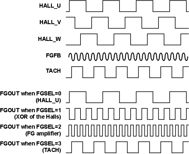 Figure 6.
7.3.3 Enable, Reset, and Clock Generation
The ENABLE pin is used to start and stop motor operation. ENABLE can be programmed to be active high or active low, depending on the state of the ENPOL bit; if ENPOL = 0, ENABLE is active high. If ENPOL = 1, the ENABLE pin is active low.
The polarity of ENABLE cannot be modified during operation through register writes; it is controlled only by the contents of the ENPOL bit in OTP memory.
When ENABLE is active, operation of the motor is enabled. When ENABLE is made inactive, the speed control loop is reset, and the motor either brakes or coasts depending on the state of the BRKMOD bit. After motor rotation has stopped (when no transitions occur on the FGOUT pin for a period of 1 s), the DRV8308 device enters a low-power standby state. In the standby state, the motor driver circuitry is disabled (all gate drive outputs are driven low, so the FET outputs are high-impedance), the gate drive regulator and charge pump are disabled, the VREG regulator and VSW power switch are disabled, and all analog circuitry is placed into a low power state. The digital circuitry in the device still operates in standby mode.
All internal logic is reset in three different ways:
- Upon device power-up.
- When VM drops below VRESET.
- When the RESET pin is high while ENABLE is active.
If RESET is high while ENABLE is inactive, then the registers read as 1. If the RESET pin is not needed, it can be connected to GND. The RESET input is deglitched with a 10-µs timer on assertion and deassertion.
An internal clock generator provides all timing for the DRV8308 device. The master oscillator runs at 100 MHz. This clock is divided to a nominal 50-MHz frequency that clocks the remainder of the digital logic.
7.3.4 Commutation
For 3-phase brushless DC motors, rotor position feedback is provided from Hall effect transducers mounted on the motor. These transducers provide three overlapping signals, each 60° apart. The windings are energized in accordance with the signals from the Hall sensors to cause the motor to move.
In addition to the Hall sensor inputs, commutation is affected by a direction control, which alters the direction of motion by reversing the commutation sequence. Control of commutation direction is by the DIRPOL register bit as well as the DIR input pin. The DIRPOL register bit is combined with the pin with an exclusive-OR function as follows:
Table 1. Direction Behavior
| DIR PIN | DIRPOL REGISTER BIT | RESULTING DIR FOR COMMUTATION |
|---|---|---|
| 0 | 0 | 0 |
| 0 | 1 | 1 |
| 1 | 0 | 1 |
| 1 | 1 | 0 |
If the commanded direction is changed while the motor is still spinning, this may cause excessive current flow in the output stage.
The DRV8308 device supports three commutation modes: standard 120° commutation using three Hall sensors, 120° commutation using a single Hall sensor, and 180° sine-wave-drive commutation.
In standard 120° commutation, mis-positioning of the Hall sensors can cause motor noise, vibration, and torque ripple. 120° commutation using a single Hall sensor (single-Hall commutation) can improve motor torque ripple and vibration because it relies on only one Hall edge for timing.
180° sine-wave-drive commutation is even more advanced, and excites the windings with a waveform that delivers nearly sinusoidal current to each winding.
7.3.4.1 120° 3-Hall Commutation
In standard 120° commutation, the motor phases are energized using simple combination logic based on all three Hall sensor inputs. Standard 120° commutation is in accordance with Table 2, Figure 7, and Figure 8:
Table 2. Standard 120° Commutation(1)
| STATE | HALL INPUTS | PRE-DRIVE OUTPUTS | ||||||||||
|---|---|---|---|---|---|---|---|---|---|---|---|---|
| DIR = 1 | DIR = 0 | PHASE U | PHASE V | PHASE W | ||||||||
| U_H | V_H | W_H | U_H | V_H | W_H | U_HSGATE | U_LSGATE | V_HSGATE | V_LSGATE | W_HSGATE | W_LSGATE | |
| 1 | L | L | H | H | H | L | L | L | PWM | L / !PWM(2) | L | H |
| 2 | L | H | H | H | L | L | PWM | L / !PWM(2) | L | L | L | H |
| 3 | L | H | L | H | L | H | PWM | L / !PWM(2) | L | H | L | L |
| 4 | H | H | L | L | L | H | L | L | L | H | PWM | L / !PWM(2) |
| 5 | H | L | L | L | H | H | L | H | L | L | PWM | L / !PWM(2) |
| 6 | H | L | H | L | H | L | L | H | PWM | L / !PWM(2) | L | L |
| 1X | H | H | H | L | L | L | L | L | L | L | L | L |
| 2X | L | L | L | H | H | H | L | L | L | L | L | L |
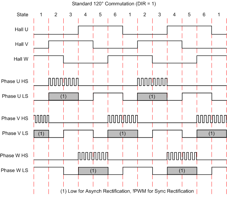 Figure 7. Standard 120° Commutation (DIR = 1)
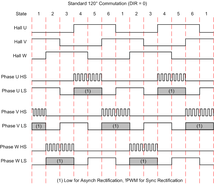 Figure 8. Standard 120° Commutation (DIR = 0)
7.3.4.2 120° Single-Hall Commutation
To generate commutation timing for single-Hall commutation, a digital timer is used to create a clock that runs at 960× the Hall sensor frequency. Only one Hall sensor input, HALL_U, is used for commutation; this eliminates any torque ripple caused by mechanical or electrical offsets of individual Hall sensors.
Single-Hall commutation is only enabled when the register BASIC = 0 and the motor is operating at a nearly constant speed or speed-locked condition. To control this function, logic is used to determine when the speed is constant and the speed control loop is locked. This logic generates the LOCK signal. The LOCK signal is also output on the LOCKn pin.
Except in PWM input modes, LOCK is also prevented from being signaled if the speed control loop integrator is saturated (either at 0 or full-scale), which indicates that the speed control loop is not locked.
Until LOCK goes active (for example, at start-up, stop, or application of a sudden load that causes motor speed to drop very quickly), standard 120° commutation is used. Because of this, three Hall sensors are required regardless of which commutation method is used.
The commutation timer drives a counter that can be offset with a value programmed in the ADVANCE register. This value allows the phase of commutation to be shifted relative to the actual Hall sensor transitions. Note that the phase advance is not functional in standard 120° commutation. The phase advance also has an automatic mode where the advance value is scaled according to motor speed (see Auto Gain and Advance Compensation).
Timing of 120° single-Hall commutation is essentially the same as standard 120° commutation shown previously. However, there are small time differences of when the transitions occur.
7.3.4.3 180° Sine-Wave-Drive Commutation
180° sine-wave-drive commutation uses a single Hall sensor to generate commutation timing, as described for 120° single-Hall commutation. In addition, the value of the commutation timer modulates the duty cycle of the outputs in accordance with a fixed pattern that approximates sinusoidal current through the windings.
The output of the commutation block is a 12-bit modulation value for each motor phase (U, V, and W) that represents the duty cycle modulation of the PWM for each output. Note that during 120° commutation, these values are either 0 or set to a constant value derived from the MOD120 register.
When using sine mode, MOD120 should be set to 3970.
 Figure 9. 180° Sine-Wave-Drive Commutation
During 180° sine-wave-drive commutation, commutation transitions occur midway between Hall transitions. The PWM duty cycle is modulated to provide sinusoidal current waveforms. Commutation (shown for asynchronous rectification) is in accordance with the table and diagrams below. Note that the diagrams show a representation of duty cycle, not level, for the PWM states.
Table 3. Commutation for Asynchronous Rectification(1)
| STATE | HALL INPUTS | PRE-DRIVE OUTPUTS | ||||||||||
|---|---|---|---|---|---|---|---|---|---|---|---|---|
| DIR = 1 | DIR = 0 | PHASE U | PHASE V | PHASE W | ||||||||
| U_H | V_H | W_H | U_H | V_H | W_H | U_HSGATE | U_LSGATE | V_HSGATE | V_LSGATE | W_HSGATE | W_LSGATE | |
| 1 | L | L | H | H | H | L | PWM | L / !PWM(2) | PWM | L / !PWM(2) | L | H |
| 2 | L | H | H | H | L | L | PWM | L / !PWM(2) | PWM | L / !PWM(2) | L | H |
| 3 | L | H | L | H | L | H | PWM | L / !PWM(2) | L | H | PWM | L / !PWM(2) |
| 4 | H | H | L | L | L | H | PWM | L / !PWM(2) | L | H | PWM | L / !PWM(2) |
| 5 | H | L | L | L | H | H | L | H | PWM | L / !PWM(2) | PWM | L / !PWM(2) |
| 6 | H | L | H | L | H | L | L | H | PWM | L / !PWM(2) | L | L / !PWM(2) |
| 1X | H | H | H | L | L | L | L | L | L | L | L | L |
| 2X | L | L | L | H | H | H | L | L | L | L | L | L |
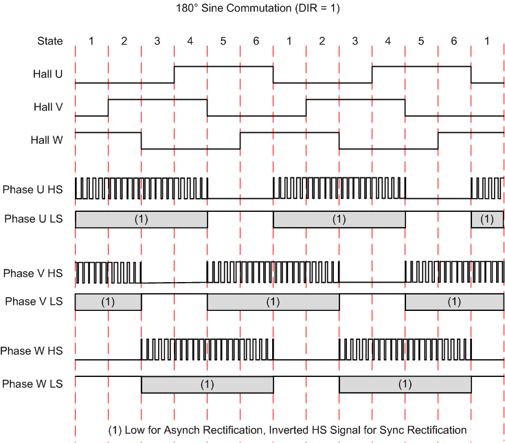 Figure 10. 180° Sine Commutation (DIR = 1)
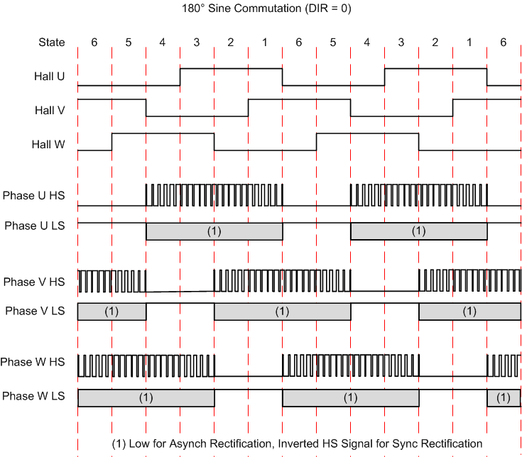 Figure 11. 180° Sine Commutation (DIR = 0)
7.3.5 Commutation Logic Block Diagram
A block diagram of the commutation logic is shown in Figure 12.
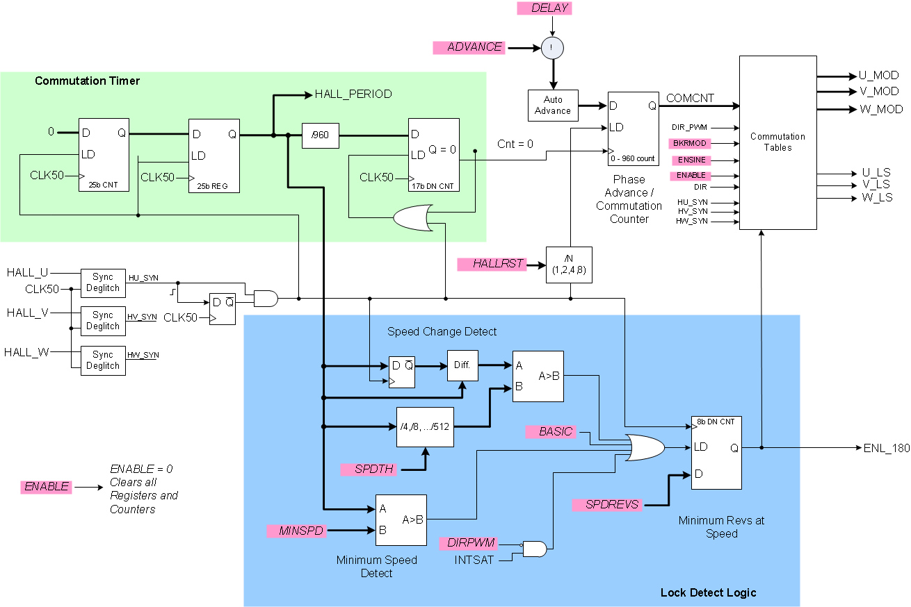 Figure 12. Commutation Logic
7.3.6 Commutation Parameters
A number of commutation parameters are programmable through registers accessed through the serial interface, including:
- ADVANCE — The phase of commutation is advanced (or delayed) relative to the Hall sensor transition by this 8-bit amount. Units are in commutation clocks, which is 1 / 960 of the HALL_U period. Note that phase advance is only applicable in single-Hall commutation modes. An automatic phase advance compensation mode can also be enabled by the AUTOADV bit (see Auto Gain and Advance Compensation for details).
- DELAY — if set, commutation is delayed relative to Hall transitions; if cleared, commutation is advanced relative to Hall transitions.
- BASIC — If set, commutation is a basic 120° 3-Hall mode with no ADVANCE.
- ENSINE — The ENSINE bit, when set, selects 180° sinusoidal commutation. The BASIC bit must also be 0.
- HALLRST — HALLRST sets how many HALL_U cycles pass for each commutation counter reset. In other words, the commutation counter is reset every N HALL_U edges. Selections available are 1, 2, 4, and 8.
- MINSPD — Sets the minimum Hall_U period that LOCK can be set. The 8-bit field represents 2.56 ms/count, with a max value of 652.8 ms.
- SPDREVS — After the MINSPD and SPEEDTH criteria are met, SPDREVS adds a minimum number of Hall_U periods that must occur for LOCK to be set.
- SPEEDTH — Sets how much speed variation is allowed across Hall_U periods while keeping LOCK set. This 3-bit field sets the percentage variation allowed by changing a programmable divider. Divisions of 1/4, 1/8, 1/16, 1/32, 1/64, 1/128, 1/256, and 1/512 are supported. These divisors correspond to 25%, 12.5%, 6.25%, 3.13%, 1.56%, 0.78%, 0.39%, and 0.20% variation per revolution.
- SPEED — In the Internal Register PWM Mode, SPEED divided by 4095 sets the input duty cycle. In Clock Frequency Mode, SPEED sets the open-loop gain during spin-up before LOCKn goes Low.
The diagram below shows how the lock parameters (MINSPD, SPEEDTH, and SPDREV) affect commutation mode.
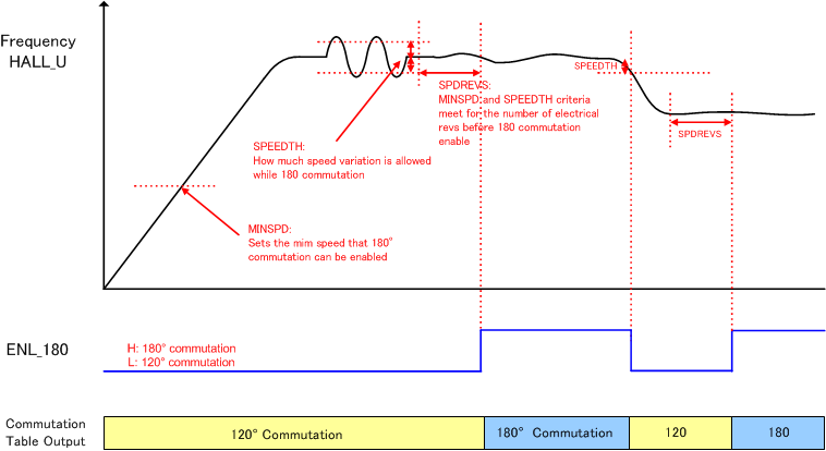 Figure 13. Commutation Parameters
7.3.7 Braking
Motor braking can be initiated by the BRKPOL register bit as well as the BRAKE pin. The BRKPOL register bit can also be used to program the polarity of the BRAKE pin, as it is combined with the pin with an exclusive-OR function as follows:
Table 4. Brake Behavior
| BRAKE PIN | BRKPOL REGISTER BIT | RESULTING FUNCTION |
|---|---|---|
| 0 | 0 | Not brake |
| 0 | 1 | Brake |
| 1 | 0 | Brake |
| 1 | 1 | Not brake |
When the motor is braking, all low-side drivers are held in an on state, causing all low-side FETs to turn on, and the integrator is reset to 0.
In addition, braking can be entered when the ENABLE pin is made inactive. BRKMOD controls the behavior of the outputs when ENABLE is inactive. If BRKMOD= 0, the outputs are 3-stated, resulting in the motor coasting; if BRKMOD = 1, all low-side FETs are turned on, causing the motor to brake.
Table 5. BRKMOD
| BRKMOD = 0 COAST |
BRKMOD = 1 BRAKE |
|
|---|---|---|
| RESET = 1 | Coast | Brake |
| BRAKE = active | Brake | Brake |
| ENABLE = inactive | Coast | Brake |
| DIR | Coast | Brake |
| Clock off | Brake | Brake |
| Power down | Coast | Brake |
7.3.8 Output Pre-Drivers
The output drivers for each phase consist of N-channel and P-channel MOSFET devices arranged as a CMOS buffer. They are designed to directly drive the gate of external N-channel power MOSFETs.
The outputs can provide synchronous or asynchronous rectification. In asynchronous rectification, only the high-side FET is turned on and off with the PWM signal; current is recirculated using external diodes, or the body diodes of the external FETs. In synchronous rectification, the low side FET is turned on when the high side is turned off.
Synchronous rectification is enabled or disabled using the SYNRECT control bit. When set to 1, synchronous rectification is used. In general, synchronous rectification results in better speed control and higher efficiency.
The high-side gate drive output UHSG is driven to VCP whenever the duty cycle output U_PD from the PWM generator is high, the enable signal U_HS from the commutation logic is active, and the current limit (VLIMITER) is not active. If the high-side FET is on and a current limit event occurs, the high-side FET is immediately turned off until the next PWM cycle.
The low-side gate drive ULSG is driven to VM whenever the internal signal U_LS is high, or whenever synchronous rectification is active and UHSG is low.
Phases V and W operate in an identical fashion.
 Figure 14. Predriver Circuit
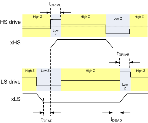 Figure 15. Drive Timing
The peak drive current of the pre-drivers is adjustable by setting the IDRIVE register bits. Peak drive currents may be set between 10 and 130 mA. Adjusting the peak current changes the output slew rate, which also depends on the FET input capacitance and gate charge.
When changing the state of the output, the peak current is applied for a short period of time (tDRIVE), to charge the gate capacitance. This time is selected by setting the TDRIVE register bits. Times of 1, 5, 10, or 15 µs may be selected. After this time, a weak current source is used to keep the gate at the desired state. When selecting the gate drive strength for a given external FET, the selected current must be high enough to fully charge and discharge the gate during the time when driven at full current, or excessive power is dissipated in the FET.
During high-side turn-on, the low-side gate is held low with a low impedance. This prevents the gate-source capacitance of the low-side FET from inducing turn-on. Similarly, during low-side turn-on, the high-side gate is held off with a low impedance.
The pre-driver circuits include enforcement of a dead time in analog circuitry, which prevents the high-side and low-side FETs from conducting at the same time. Additional dead time can be added (in digital logic) by setting the DTIME register bits.
7.3.9 Current Limit
The current limit circuit activates if the voltage detected across the low-side sense resistor exceeds VLIMITER. This feature restricts motor current to less than VLIMITER/RISENSE, and it reduces the requirements of the external power supply. Note that the current limit circuit is ignored immediately after the PWM signal goes active for a short blanking time, to prevent false trips of the current limit circuit.
If current limit activates, the high-side FET is disabled until the beginning of the next PWM cycle. If synchronous rectification is enabled when the current limit activates, the low-side FET is activated while the high-side FET is disabled.
7.3.10 Charge Pump
Since the output stages use N-channel FETs, a gate drive voltage higher than the VM power supply is needed to fully enhance the high-side FETS. The DRV8308 device integrates a charge pump circuit that generates a voltage approximately 10 V more than the VM supply for this purpose.
The charge pump requires two external capacitors for operation. For details on these capacitors (value, connection, and so forth), refer to the Pin Functions table in the Pin Configurations and Functions section.
The charge pump is shutdown when in standby mode (ENABLE inactive).
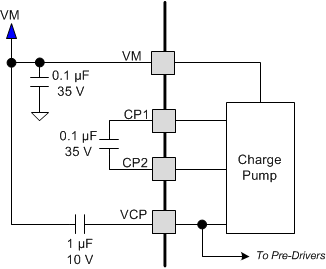 Figure 16. Charge Pump
7.3.11 5-V Linear Regulator
A 5-V linear regulator (VREG) is provided to power internal logic and external circuitry, such as the Hall effect sensors.
A capacitor must be connected from the VREG output to ground, even if the output is not used for external circuitry. The recommended capacitor value is a 0.1-μF, 10-V ceramic capacitor.
The VREG output is designed to provide up to 30-mA output current, but power dissipation and thermal conditions must be considered. As an example, with 24 V in and 20 mA out, power dissipated in the linear regulator is 19 V × 20 mA = 380 mW.
The VREG regulator is shutdown in standby mode (when ENABLE is inactive).
7.3.12 Power Switch
A low-current switch is provided in the DRV8308 device that can be used to power the Hall sensors or other external circuitry through the VSW pin. When ENABLE is active the switch is turned on, connecting the VSW pin to VM. When ENABLE is inactive the switch is turned off (standby mode).
7.3.13 Protection Circuits
A number of protection circuits are included in the DRV8308 device. Faults are reported by asserting the FAULTn pin (an active-low, open-drain output signal), as well as setting the appropriate bit or bits in the FAULT register. Note that bits in the FAULT register remain set until either a 0 is written to them, RESET is asserted, or the device power is cycled.
7.3.13.1 VM Undervoltage Lockout (UVLO)
If the VM power supply drops, there may not be enough voltage to fully turn on the output FETs. Operation in this condition causes excessive heating in the output FETs. To protect against this, the DRV8308 device contains an undervoltage lockout circuit.
In the event that the VM supply voltage drops below the undervoltage lockout threshold (VUVLO), the FAULTn pin is driven active and the motor driver is disabled. After VM returns to a voltage above the undervoltage lockout threshold, the FAULTn pin is high impedance and operation of the motor driver automatically resumes.
The UVLO bit in the FAULT register is set. This bit remains set until a 0 is written to the UVLO bit.
At power-up, the UVLO bit is set.
Note that register reads and writes are still possible during the UVLO condition, as long as VM stays above the VM reset threshold. If VM drops below the VM reset threshold, all registers are reset and register read or write is not functional.
7.3.13.2 VM Overvoltage (VMOV)
In some cases, if synchronous rectification is used, energy from the mechanical system can be forced back into the VM power supply. This can result in the VM power supply being boosted by the energy in the mechanical system, causing breakdown of the output FETs, or damaging the DRV8308 device. To protect against this, the DRV8308 device has overvoltage protection.
There are two overvoltage thresholds, selectable by the OVTH bit. An overvoltage event is recognized if the VM voltage exceeds the selected overvoltage threshold (VMOVLO). Note that for the output FETs to be protected, they must be rated for a voltage greater than the selected overvoltage threshold.
In the event of an overvoltage, the FAULTn pin is pulled low. If synchronous rectification is enabled, the output stage is forced into asynchronous rectification. After VM returns to a voltage below the overvoltage threshold, the FAULTn pin is high impedance. If synchronous rectification was enabled prior to the overvoltage event, after a fixed 60-µs delay, synchronous rectification is re-enabled.
The VMOV bit in the FAULT register is set. This bit remains set until a 0 is written to the VMOV bit.
7.3.13.3 Motor Overcurrent (OCP)
Overcurrent protection (OCP) is provided on each FET in addition to the current limit circuit. The OCP circuit is designed to protect the output FETs from atypical conditions such as a short circuit between the motor outputs and each other, power, or ground.
The OCP circuit is independent from the current limit circuitry. OCP works by monitoring the voltage drop across the external FETs when they are enabled. If the voltage across a driven FET exceeds VFETOCP for more than tOCP an OCP event is recognized. VFETOCP is configurable by register OCPTH and tOCP is configurable by register OCPDEG.
In addition to monitoring the voltage across the FETs, an OCP event is triggered if the voltage applied to the ISEN pin exceeds the VSENSEOCP threshold voltage.
In the event of an OCP event, FAULTn is pulled low, and the motor driver is disabled.
After a fixed delay of 5 ms, the FAULTn pin is driven inactive and the motor driver is re-enabled.
The OCP bit in the FAULT register is set when an OCP event is recognized. This bit remains set until a 0 is written to the OCP bit.
7.3.13.4 Charge Pump Failure (CPFAIL)
If the voltage generated by the high-side charge pump is too low, the high-side output FETs are not fully turned on, and excessive heating results. To protect against this, the DRV8308 device has a circuit that monitors the charge pump voltage.
If the charge pump voltage drops below VCPFAIL, the FAULTn pin is pulled low and the motor driver is disabled. After the charge pump voltage returns to a voltage above the VCPFAIL threshold, the FAULTn pin is high impedance and operation of the motor driver automatically resumes.
The CPFAIL bit in the FAULT register is set when the charge pump voltage drops below VCPFAIL. This bit remains set until a 0 is written to the CPFAIL bit.
At power-up, the CPFAIL bit is set.
7.3.13.5 Charge Pump Short (CPSC)
To protect against excessive power dissipation inside the DRV8308 device, a circuit monitors the charge pump and disables it in the event of a short circuit on the PCB.
If a short circuit is detected on the charge pump, the FAULTn pin is pulled low and the motor driver is disabled. After a fixed period of 5 s, the FAULTn pin is high impedance and operation of the motor driver automatically resumes. If the short circuit condition is still present, the cycle repeats.
The CPSC bit in the FAULT register is set when a short circuit is detected on the charge pump. This bit remains set until a 0 is written to the CPSC bit.
7.3.13.6 Overtemperature (OTS)
To protect against any number of faults that could result in excessive power dissipation inside the device, the DRV8308 device includes overtemperature protection.
Overtemperature protection activates if the temperature of the die exceeds the OTS threshold temperature (TTSD). If this occurs, the FAULTn pin is pulled low, the device is disabled and the OTS bit in the FAULT register is set. This OTS bit remains set until a 0 is written to the OTS bit.
If the RETRY bit is set after the temperature has fallen below the OTS threshold, the part re-enables itself after a fixed delay of 5 s.
If the RETRY bit is not set, the part disables the pre-drivers until RESET is asserted, or until power has been removed and re-applied to the device.
7.4 Device Functional Modes
7.4.1 Modes of Speed Input
The DRV8308 device is designed to support a wide range of motor speeds and constructions. Speeds of up to approximately 50000 RPM are supported with motor constructions of up to 16 poles, or corresponding lower speeds with more poles. This translates into a Hall sensor speed of up to 6.7 kHz. (The frequency of one Hall sensor can be calculated by RPM × (motor poles) / 120.)
Speed control of the motor is accomplished by varying the duty cycle applied to the external FETs. Three methods of speed control input are possible with the DRV8308 device:
- Clock Frequency Mode: This is closed-loop speed control that locks the FGOUT frequency with the CLKIN frequency.
- Clock PWM Mode: This is open-loop, where the duty cycle of the clock on CLKIN scales the speed of the motor.
- Internal Register PWM Mode: This is open-loop, where register SPEED divided by 4095 commands the input duty cycle.
The mode used is set by the SPDMODE register.
7.4.1.1 Clock Frequency Mode
For a practical guide on tuning closed-loop speed control, refer to Section 3 of theDRV8308EVM User's Guide.
In Clock Frequency Mode, the clock signal is deglitched by the 51.2-MHz clock. The deglitched input, along with the FG signal (derived from the FG amplifier, TACH input, or the Hall sensors), are input to a speed differentiator, where the CLKIN signal is compared to the actual speed of the motor (determined by the FG frequency). The speed differentiator outputs are UP and DOWN pulses.
The deglitcher and speed differentiator are shown in Figure 17:
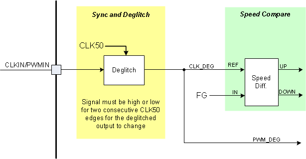 Figure 17. Deglitcher and Speed Differentiator
The UP and DOWN outputs of the speed differentiator are integrated by accumulating the value set by the SPDGAIN register for each cycle of the integrator clock (CLK50 divided by the value of the INTCLK register) that an UP or DOWN signal is active. If UP is active, the amount is added to the current integrator output; if the DOWN input is active, the value is subtracted. If neither signal is active, the integrator output remains the same. Note that the integrator output is reset to 0 at any time the motor is disabled or in brake, and at reset. The integrator output does not roll over at maximum or minimum count.
At the moment that ENABLE is made active, the integrator and filters are reset to 0. If there are no transitions on the CLKIN pin, no UP pulses are generated, so the integrator remains at 0, and the motor is not driven.
Once the motor is running, if the signal on CLKIN stops, DOWN pulses are generated until the integrator reaches 0. This actively decelerates the motor (brake) until the motor stops.
The output of the integrator is applied to a programmable digital filter. The filter has one pole and one zero. The pole location is programmable from approximately 100 to 1600 Hz, and is set via the FILK1 register; the zero location is programmable from 2 to 100 Hz and is set via the FILK2 register. The filter may be bypassed by setting the BYPFILT bit.
For a given pole and zero frequency, FILK1 and FILK2 are calculated as follows:

where
- fz is the desired zero frequency
- fp is the desired pole frequency
- fs is the filter sample rate (195000 Hz)
- The result is rounded to the nearest integer
Following the filter is a programmable lead compensator, which also contains one pole and one zero. The compensator characteristics are programmable by the COMPK1 and COMPK2 registers. Center frequency is programmable between 20 and 100 Hz, with a phase lead between 0° and 80°. The compensator may be bypassed by setting the BYPCOMP bit.
For a given pole and zero frequency, COMPK1 and COMPK2 are calculated as follows:

where
- fz is the desired zero frequency
- fp is the desired pole frequency
- fs is the filter sample rate (195000 Hz)
- The result is rounded to the nearest integer
The filter and compensator ratios also scale DC gain in the same way as LOOPGAIN. DC gain is scaled by 2×(FILK2/FILK1) and 0.5×(COMPK2/COMPK1).
The digital filter and compensator are reset to 0 whenever the motor is disabled.
The integrator, filter, and lead compensator result in a typical open-loop response as shown in Figure 18. Note that the locations of the poles and zeros are not restricted to what is shown.
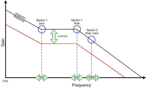 Figure 18. Open-Loop Response
The integrator operates on the periods of CLKIN and the Feedback as shown in Figure 19:
 Figure 19. Integrator and Filters
7.4.1.2 Clock PWM and Internal Register PWM Modes
In PWM input modes, the PWM input signal is timed using a 50 MHz clock to generate a 12-bit number that corresponds to the duty cycle of the incoming PWM signal. The input PWM frequency should be between 16 and 50 kHz, higher PWM frequencies work, but resolution is degraded. Note that the gate driver’s output PWM frequency is independent of the speed control PWM input frequency; the output PWM frequency is selected by the PWMF register bits.
The measured input duty cycle is scaled by the contents of the MOD120 register. With a full-scale MOD120 register (4095 decimal), the output duty cycle is 2× the input duty cycle. To make the output duty cycle equal to the input, a value of 2048 decimal should be written to MOD120.
An additional multiplication factor of 2 is introduced when the BYPCOMP bit is set; if BYPCOMP is set, the output duty cycle is 4× the input duty cycle (when MOD120 is 4095).
In register speed control mode, a 12-bit register SPEED is used to directly provide the speed command.
During sine commutation, the input duty cycle is multiplied by the modulation values for each phase (MOD_U, MOD_V, and MOD_W) to generate a 12-bit value that determines the output PWM duty cycle of each phase. Note that in 120° commutation, the MOD values are fixed at a duty cycle that is set by the MOD120 register.
The PWM frequency can be set to either 25, 50, 100, or 200 kHz, with register PWMF. Lower PWM frequencies are desirable to minimize switching losses; higher PWM frequencies provide better control resolution, especially at very high motor speeds.
The outputs of the PWM generators are the signals U_PD, V_PD, and W_PD. These contain the duty cycle information for each phase.
Modulation and PWM generation is shown in Figure 20:
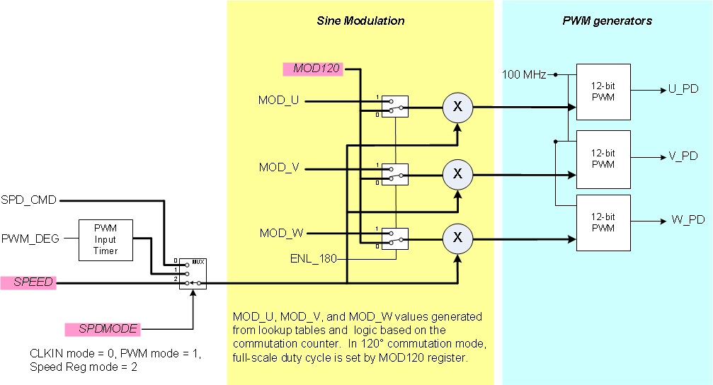 Figure 20. Modulation and PWM Generation
7.4.2 Auto Gain and Advance Compensation
The DRV8308 device provides modes to automatically scale the loop gain and the phase advance settings based on motor speed. This helps improve loop stability and motor performance in cases where the motor must operate over a wide speed range with a single set of parameters. For applications that run at only one speed, these functions should be left disabled.
Auto gain compensation is enabled by setting the AUTOGAIN bit. Auto gain will scale the LOOPGAIN of the system using the following equation:
Automatic advance is enabled by setting the AUTOADV bit. The advance setting is scaled such that at zero speed, there is no phase advance. As speed increases, the phase advance is increased using the equation below:
Both the gain and advance values are latched when LOCK goes active (when the motor is at constant speed).
The auto gain and advance functions are shown in Figure 21:
 Figure 21. Auto Gain and Advance Functions
7.4.3 External EEPROM Mode
A serial EEPROM can be connected to the serial port to load the register contents. To activate external EEPROM mode, connect the SMODE pin to logic high. This causes the SPI interface to act as a master, and load data from an external EEPROM. The DRV8308 device latches data on the falling edge of SCLK.
The serial EEPROM should be a microwire-compatible, 16-bit-word device, such as the 93C46B. The VREG power supply can be used to power the EEPROM. Connections are as shown in Figure 22:
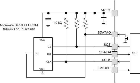 Figure 22. EEPROM Mode Connections
Data in the EEPROM should be arranged starting at address 0 exactly as shown in Table 6. EEPROM data bits 12 to 15 are unused.
To program the EEPROM device in-circuit while connected to the DRV8308 device, place the DRV8308 device into the reset state by driving RESET high. This 3-states the serial interface pins and allows them to be overdriven by external programming logic. Alternatively, the EEPROM may be programmed off-board before assembly. The DRV8308 device cannot program an EEPROM.
7.5 Programming
7.5.1 Serial Interface
A simple SPI serial interface is used to write to the control registers in the DRV8308 device. Optionally, the interface can be configured to automatically load the registers from an external EEPROM device.
Data is shifted into a holding register when SCS is active high. When SCS is returned to inactive (low), the data received is latched into the addressed register.
7.5.2 Serial Data Format
The serial data consists of a 24-bit serial write, with a read or write bit, 7 address bits, and 16 data bits. The address bits identify one of the registers defined in Table 8.
To write to a register, data is shifted in after the address as shown in Figure 23:

Data may be read from the registers through the SDATO pin. During a read operation, only the address is used from the SDATI pin; the data bits following are ignored. Reading is enabled by setting the READ bit at the beginning of the access:

7.5.3 Programming the OTP Configuration Memory
To permanently program the non-volatile OTP memory, first write all the data into the registers as described previously, and then follow this sequence:
Table 6. Programming the OTP Configuration Memory
| ADDRESS | DATA | ACTION |
|---|---|---|
| -- | -- | device ENABLE must be active |
| 0x2D | 0x1213 | write |
| 0x2D | 0x1415 | write |
| 0x2D | 0x1617 | write |
| 0x2D | 0x1819 | write |
| 0x39 | 0x0002 | write |
| -- | -- | wait 10 ms minimum |
| 0x2D | 0EDD | write |
The internal OTP memory can only be programmed once. After programming, the registers can still be overwritten by accesses through the SPI port, or by using an external EEPROM.
7.6 Register Map
7.6.1 Control Registers
The DRV8308 device uses internal registers to set operation parameters, including the characteristics of the speed control loop, commutation settings, gate drive current, and so forth. The registers are programmed through a serial SPI communications interface. In addition, the registers can be permanently programmed into non-volatile OTP memory, or loaded from an external serial EEPROM device.
Table 7 is the register map for the device.
Table 7. Control Register Map
| Address | Bit 15 | Bit 14 | Bit 13 | Bit 12 | Bit 11 | Bit 10 | Bit 9 | Bit 8 | Bit 7 | Bit 6 | Bit 5 | Bit 4 | Bit 3 | Bit 2 | Bit 1 | Bit 0 |
|---|---|---|---|---|---|---|---|---|---|---|---|---|---|---|---|---|
| 0x00 | AG_SETPT | ENPOL | DIRPOL | BRKPOL | SYNRECT | PWMF | SPDMODE | FGSEL | BRKMOD | RETRY | ||||||
| 0x01 | RSVD | ADVANCE | ||||||||||||||
| 0x02 | SPDREVS | MINSPD | ||||||||||||||
| 0x03 | BASIC | SPEEDTH | MOD120 | |||||||||||||
| 0x04 | RSVD | HALLRST | DELAY | AUTOADV | AUTOGAIN | ENSINE | TDRIVE | DTIME | IDRIVE | |||||||
| 0x05 | RSVD | INTCLK | SPDGAIN | |||||||||||||
| 0x06 | HALLPOL | RSVD | BYPFILT | FILK1 | ||||||||||||
| 0x07 | RSVD | FILK2 | ||||||||||||||
| 0x08 | RSVD | BYPCOMP | COMK1 | |||||||||||||
| 0x09 | AA_SETPT | COMK2 | ||||||||||||||
| 0x0A | OCPDEG | OCPTH | OVTH | VREG_EN | LOOPGAIN | |||||||||||
| 0x0B | RSVD | SPEED | ||||||||||||||
| 0x2A | RSVD | VMOV | CPFAIL | UVLO | OTS | CPOC | OCP | |||||||||
At power-up, when VM rises above the VM reset threshold, or whenever RESET is toggled, the register contents are loaded from the OTP memory or EEPROM (depending on SMODE). For details on external EEPROM connections, see External EEPROM Mode. If the OTP has not been programmed and the DRV8308 device is powered-up with SMODE low, the default register values are all 0, except for the FAULT register, which defaults to 0x18. FAULT bits can be cleared by writing 0.
At any time, the register contents may be written or overwritten through the SPI interface.
For detailed descriptions for each register, refer to the prior sections.
Table 8. Register Descriptions
| ADDRESS | BIT | NAME | DESCRIPTION | TYPE(1) | |||
|---|---|---|---|---|---|---|---|
| 0x00 | 15:12 | AG_SETPT | Autogain Setpoint | RW | |||
| 0000 = 3 Hz 0001 = 6 Hz 0010 = 12 Hz 0011 = 24 Hz |
0100 = 48 Hz 0101 = 95 Hz 0110 = 191 Hz 0111 = 382 Hz |
1000 = 763 Hz 1001 = 1.5 kHz 1010 = 3 kHz 1011 = 6 kHz |
1100 = 12 kHz 1101 = 24 kHz 1110 = 49 kHz 1111 = 98 kHz |
||||
| 11 | ENPOL | ENABLE pin polarity | RW | ||||
| 0 = Device is active when ENABLE is high 1 = Device is active when ENABLE is low |
|||||||
| 10 | DIRPOL | DIR pin polarity | RW | ||||
| 0 = Normal DIR pin behavior 1 = Inversed DIR pin behavior |
|||||||
| 9 | BRKPOL | BRAKE pin polarity | RW | ||||
| 0 = Brake when BRAKE is high 1 = Brake when BRAKE is low |
|||||||
| 8 | SYNRECT | Synchronous rectification | RW | ||||
| 0 = Disabled 1 = Enabled |
|||||||
| 7:6 | PWMF | The PWM frequency used on the external FETs | RW | ||||
| 00 = 25 kHz 01 = 50 kHz 10 = 100 kHz 11 = 200 kHz |
|||||||
| 5:4 | SPDMODE | Speed control mode | RW | ||||
| 00 = Clock Frequency Mode 01 = Clock PWM Mode 10 = Internal Register PWM Mode 11 = Reserved |
|||||||
| 3:2 | FGSEL | FG select | RW | ||||
| 00 = Use HALL_U to generate FG 01 = Use XOR of all three Hall sensors 10 = Use FG amplifier input 11 = Use TACH input signal |
|||||||
| 1 | BRKMOD | Motor brake mode | RW | ||||
| 0 = Coast when ENABLE is inactive (outputs 3-state) 1 = Brake when ENABLE is inactive (all low-side FETs on) |
|||||||
| 0 | RETRY | Retry mode | RW | ||||
| 0 = Latch off in case of fault 1 = Automatic retry in case of fault |
|||||||
| 0x01 | 15:8 | RSVD | Reserved | – | |||
| 7:0 | ADVANCE | Commutation timing advance versus Hall signals; each count is 1 / 960 the Hall_U period | RW | ||||
| 0x02 | 15:8 | SPDREVS | After the MINSPD and SPEEDTH criteria are met, SPDREVS adds a minimum number of Hall_U periods that must occur for LOCK to be set | RW | |||
| 7:0 | MINSPD | Sets the minimum Hall_U period that LOCK can be set; each count is 2.56 ms | RW | ||||
| 0x03 | 15 | BASIC | Basic operation | RW | |||
| 0 = Normal device operation 1 = Disables ADVANCE functionality and forces 3-Hall 120° commutation |
|||||||
| 14:12 | SPEEDTH | Speed change tolerance for LOCK | RW | ||||
| 000 = 1/512 rev (0.20%) 001 = 1/256 rev (0.39%) 010 = 1/128 rev (0.78%) |
011 = 1/64 rev (1.56%) 100 = 1/32 rev (3.13%) 101 = 1/16 rev (6.25%) |
110 = 1/8 rev (12.5%) 111 = 1/4 rev (25%) |
|||||
| 11:0 | MOD120 | Scales the input duty cycle in PWM modes | RW | ||||
| 0x04 | 15:14 | RSVD | Reserved | RW | |||
| 13:12 | HALLRST | Sets the frequency to reset the Hall commutation counter | RW | ||||
| 00 = Every Hall_U cycle 01 = Every 2nd Hall_U cycle 10 = Every 4th Hall_U cycle 11 = Every 8th Hall_U cycle |
|||||||
| 11 | DELAY | Controls whether ADVANCE leads or lags Hall signals | RW | ||||
| 0 = Commutate before Hall signals arrive 1 = Commutate after Hall signals arrive |
|||||||
| 10 | AUTOADV | Enables automatic advance compensation | RW | ||||
| 0 = Disabled 1 = Enabled |
|||||||
| 9 | AUTOGAIN | Enables automatic gain compensation | RW | ||||
| 0 = Disabled 1 = Enabled |
|||||||
| 8 | ENSINE | Enables 180° sine wave current drive | RW | ||||
| 0 = Disabled 1 = Enabled |
|||||||
| 7:6 | TDRIVE | Predriver high-current drive time | RW | ||||
| 00 = 1 µs 01 = 5 µs 10 = 10 µs 11 = 15 µs |
|||||||
| 5:3 | DTIME | Additional dead time added between high-side and low-side driving (typical) | RW | ||||
| 000 = 60 ns 001 = 120 ns 010 = 240 ns |
011 = 500 ns 100 = 740 ns 101 = 1.0 µs |
110 = 1.24 µs 111 = 1.5 µs |
|||||
| 2:0 | IDRIVE | Predriver output peak current | RW | ||||
| 000 = 10 mA 001 = 20 mA 010 = 30 mA |
011 = 50 mA 100 = 90 mA 101 = 100 mA |
110 = 110 mA 111 = 130 mA |
|||||
| 0x05 | 15 | RSVD | Reserved | – | |||
| 14:12 | INTCLK | Integrator clock frequency | RW | ||||
| 000 = 50 MHz 001 = 25 MHz 010 = 12.5 MHz |
011 = 6.3 MHz 100 = 3.1 MHz 101 = 1.6 MHz |
110 = 0.8 MHz 111 = 0.4 MHz |
|||||
| 11:0 | SPDGAIN | Speed compensator gain | RW | ||||
| 0x06 | 15 | HALLPOL | Hall polarity | RW | |||
| 0 = Hall signal logic levels are directly used 1 = Hall signal logic levels are inverted |
|||||||
| 14:13 | RSVD | Reserved | – | ||||
| 12 | BYPFILT | Bypass the filter that FILK1 and FILK2 configure | RW | ||||
| 0 = Filter is enabled 1 = Filter is disabled (FILK1 and FILK2 are ignored) |
|||||||
| 11:0 | FILK1 | Filter coefficient that sets the pole frequency | RW | ||||
| 0x07 | 15:12 | RSVD | Reserved | – | |||
| 11:0 | FILK2 | Filter coefficient that sets the zero frequency | RW | ||||
| 0x08 | 15:13 | RSVD | Reserved | – | |||
| 12 | BYPCOMP | Bypass the compensator (COMPK1 and COMPK2 are ignored) | RW | ||||
| 0 = Filter is enabled 1 = Filter is disabled (FILK1 and FILK2 are ignored) |
|||||||
| 11:0 | COMPK1 | Compensator coefficient that sets the pole frequency | RW | ||||
| 0x09 | 15:12 | AA_SETPT | Autoadvance setpoint | RW | |||
| 0000 = 3 Hz 0001 = 6 Hz 0010 = 12 Hz 0011 = 24 Hz |
0100 = 48 Hz 0101 = 95 Hz 0110 = 191 Hz 0111 = 382 Hz |
1000 = 763 Hz 1001 = 1.5 kHz 1010 = 3 kHz 1011 = 6 kHz |
1100 = 12 kHz 1101 = 24 kHz 1110 = 49 kHz 1111 = 98 kHz |
||||
| 11:0 | COMPK2 | Compensator coefficient that sets the zero frequency | RW | ||||
| 0x0A | 15:14 | OCPDEG | Overcurrent protection deglitch time to ignore voltage spikes. Controls tOCP and tBLANK. | RW | |||
| 00: tocp = 1.6µs, tBLANK = 2µs 01: tocp = 2.3µs, tBLANK = 3µs 10: tocp = 3µs, tBLANK = 3.75µs 11: tocp = 5µs, tBLANK = 6µs |
|||||||
| 13:12 | OCPTH | Protection threshold for VFETOCP | RW | ||||
| 00 = 250 mV 01 = 500 mV 10 = 750 mV 11 = 1000 mV |
|||||||
| 11 | OVTH | Protection threshold for VOVLO | RW | ||||
| 0 = 34.5 V 1 = 28 V |
|||||||
| 10 | VREG_EN | Writing this bit over SPI requires ENABLE to be active. | RW | ||||
| 0 = VREG is enabled only when ENABLE is active 1 = VREG is always enabled |
|||||||
| 9:0 | LOOPGAIN | Sets the overall gain for the speed control loop | RW | ||||
| 0x0B | 15:12 | RSVD | Reserved | – | |||
| 11:0 | SPEED | In the Internal Register PWM Mode, SPEED divided by 4095 sets the input duty cycle. In Clock Frequency Mode, SPEED sets the open-loop gain during spin-up before LOCKn goes Low. | RW | ||||
| 0x2A | 15:7 | RSVD | Reserved | – | |||
| 6 | RSVD | Reserved | RW | ||||
| 5 | VMOV | Fault: VM overvoltage | RW | ||||
| 0 = Normal 1 = Fault detected |
|||||||
| 4 | CPFAIL | Fault: charge pump undervoltage | RW | ||||
| 0 = Normal 1 = Fault detected (default on power up) |
|||||||
| 3 | UVLO | Fault: VM undervoltage | RW | ||||
| 0 = Normal 1 = Fault detected (default on power up) |
|||||||
| 2 | OTS | Fault: overtemperature shutdown | RW | ||||
| 0 = Normal 1 = Fault detected |
|||||||
| 1 | CPOC | Fault: charge pump overcurrent | RW | ||||
| 0 = Normal 1 = Fault detected |
|||||||
| 0 | OCP | Fault: motor OCP | RW | ||||
| 0 = Normal 1 = Fault detected |
|||||||