ZHCSKV7A November   2020  – July 2022 DLP500YX

PRODUCTION DATA  

  1. 特性
  2. 应用
  3. 说明
  4. Revision History
  5. Pin Configuration and Functions
  6. Specifications
    1. 6.1  Absolute Maximum Ratings
    2. 6.2  Storage Conditions
    3. 6.3  ESD Ratings
    4. 6.4  Recommended Operating Conditions
    5. 6.5  Thermal Information
    6. 6.6  Electrical Characteristics
    7. 6.7  Capacitance at Recommended Operating Conditions
    8. 6.8  Timing Requirements
    9. 6.9  Typical Characteristics
    10. 6.10 System Mounting Interface Loads
    11. 6.11 Micromirror Array Physical Characteristics
    12. 6.12 Micromirror Array Optical Characteristics
    13. 6.13 Window Characteristics
    14. 6.14 Chipset Component Usage Specification
  7. Detailed Description
    1. 7.1 Overview
    2. 7.2 Functional Block Diagram
    3. 7.3 Feature Description
      1. 7.3.1 Power Interface
      2. 7.3.2 Timing
    4. 7.4 Device Functional Modes
    5. 7.5 Optical Interface and System Image Quality Considerations
      1. 7.5.1 Numerical Aperture and Stray Light Control
      2. 7.5.2 Pupil Match
      3. 7.5.3 Illumination Overfill
    6. 7.6 Micromirror Array Temperature Calculation
      1. 7.6.1 Micromirror Array Temperature Calculation using Illumination Power Density
      2. 7.6.2 Micromirror Array Temperature Calculation using Total Illumination Power
      3. 7.6.3 Micromirror Array Temperature Calculation using Screen Lumens
    7. 7.7 Micromirror Landed-On/Landed-Off Duty Cycle
      1. 7.7.1 Definition of Micromirror Landed-On/Landed-Off Duty Cycle
      2. 7.7.2 Landed Duty Cycle and Useful Life of the DMD
      3. 7.7.3 Landed Duty Cycle and Operational DMD Temperature
      4. 7.7.4 Estimating the Long-Term Average Landed Duty Cycle of a Product or Application
  8. Application and Implementation
    1. 8.1 Application Information
    2. 8.2 Typical Application
      1. 8.2.1 Design Requirements
      2. 8.2.2 Detailed Design Procedure
    3. 8.3 DMD Die Temperature Sensing
  9. Power Supply Recommendations
    1. 9.1 DMD Power Supply Power-Up Procedure
    2. 9.2 DMD Power Supply Power-Down Procedure
    3. 9.3 Restrictions on Hot Plugging and Hot Swapping
      1. 9.3.1 No Hot Plugging
      2. 9.3.2 No Hot Swapping
      3. 9.3.3 Intermittent or Voltage Power Spike Avoidance
  10. 10Layout
    1. 10.1 Layout Guidelines
      1. 10.1.1 Critical Signal Guidelines
      2. 10.1.2 Power Connection Guidelines
      3. 10.1.3 Noise Coupling Avoidance
    2. 10.2 Layout Example
      1. 10.2.1 Layers
      2. 10.2.2 Impedance Requirements
      3. 10.2.3 Trace Width, Spacing
        1. 10.2.3.1 Voltage Signals
  11. 11Device and Documentation Support
    1. 11.1 第三方产品免责声明
    2. 11.2 Device Support
      1. 11.2.1 Device Nomenclature
      2. 11.2.2 Device Markings
    3. 11.3 Documentation Support
      1. 11.3.1 Related Documentation
    4. 11.4 接收文档更新通知
    5. 11.5 支持资源
    6. 11.6 Trademarks
    7. 11.7 Electrostatic Discharge Caution
    8. 11.8 术语表
  12. 12Mechanical, Packaging, and Orderable Information

封装选项

机械数据 (封装 | 引脚)
散热焊盘机械数据 (封装 | 引脚)
订购信息

DMD Die Temperature Sensing

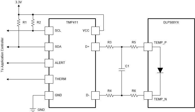
The DMD features a built-in thermal diode that measures the temperature at one corner of the die outside the micromirror array. The DMD thermal diode pins B17 and B18 can be connected to the TMP411 temperature sensor as shown in Figure 8-2, and an external processor can interface with the TMP411 temperature sensor over I2C bus to allow monitoring of the DMD temperature. This temperature data can be leveraged to incorporate additional functionality in the overall system design such as adjusting illumination, fan speeds, and so forth, all with the idea of maintaining appropriate temperature control of the DMD.
GUID-70F184DF-4AB9-4A15-951B-2F6BEC6A045E-low.gif
Details omitted for clarity, see the DLPLCR500YXEVM evaluation module design for connections.
See the TMP411 datasheet for system board layout recommendation.
See the TMP411 datasheet and the DLPLCR500YXEVM evaluation module design for suggested component values for R1, R2, R3, R4, and C1.
R5 = 0 Ω. R6 = 0 Ω. Zero ohm resistors need to be located close to the DMD package pins.
Figure 8-2 TMP411 Sample Schematic