ZHCSQO2L august   1998  – september 2023 CD4051B , CD4052B , CD4053B

PRODUCTION DATA  

  1.   1
  2. 特性
  3. 应用
  4. 说明
  5. Revision History
  6. Pin Configuration and Functions
  7. Specifications
    1. 6.1 Absolute Maximum Ratings
    2. 6.2 ESD Ratings
    3. 6.3 Recommended Operating Conditions
    4. 6.4 Thermal Information
    5. 6.5 Electrical Characteristics
    6. 6.6 AC Performance Characteristics
    7. 6.7 Typical Characteristics
  8. Parameter Measurement Information
  9. Detailed Description
    1. 8.1 Overview
    2. 8.2 Functional Block Diagrams
    3. 8.3 Feature Description
    4. 8.4 Device Functional Modes
  10. Application and Implementation
    1. 9.1 Application Information
    2. 9.2 Typical Application
      1. 9.2.1 Design Requirements
      2. 9.2.2 Detailed Design Procedure
      3. 9.2.3 Application Curve
    3. 9.3 Power Supply Recommendations
    4. 9.4 Layout
      1. 9.4.1 Layout Guidelines
      2. 9.4.2 Layout Example
  11. 10Device and Documentation Support
    1. 10.1 Documentation Support
      1. 10.1.1 Related Documentation
    2. 10.2 接收文档更新通知
    3. 10.3 支持资源
    4. 10.4 Trademarks
    5. 10.5 静电放电警告
    6. 10.6 术语表
  12. 11Mechanical, Packaging, and Orderable Information

封装选项

机械数据 (封装 | 引脚)
散热焊盘机械数据 (封装 | 引脚)
订购信息

Functional Block Diagrams

GUID-19BF9958-5DDA-48C4-A736-3904B5D414A2-low.gif
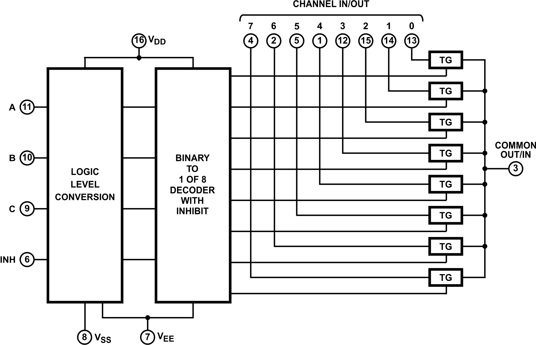
All inputs are protected by standard CMOS protection network.
Figure 8-1 Functional Block Diagram, CD4051B
GUID-7DAA2A39-8C1F-4418-825E-9D9323A7E34C-low.gif
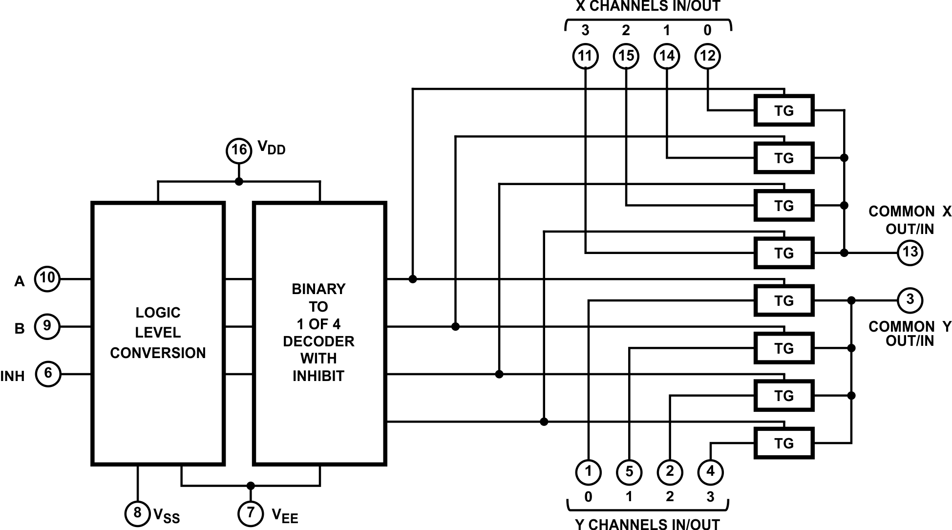
All inputs are protected by standard CMOS protection network.
Figure 8-2 Functional Block Diagram, CD4052B
GUID-10FFD2B9-B433-4E48-BA72-8A0F3625BCD5-low.gif
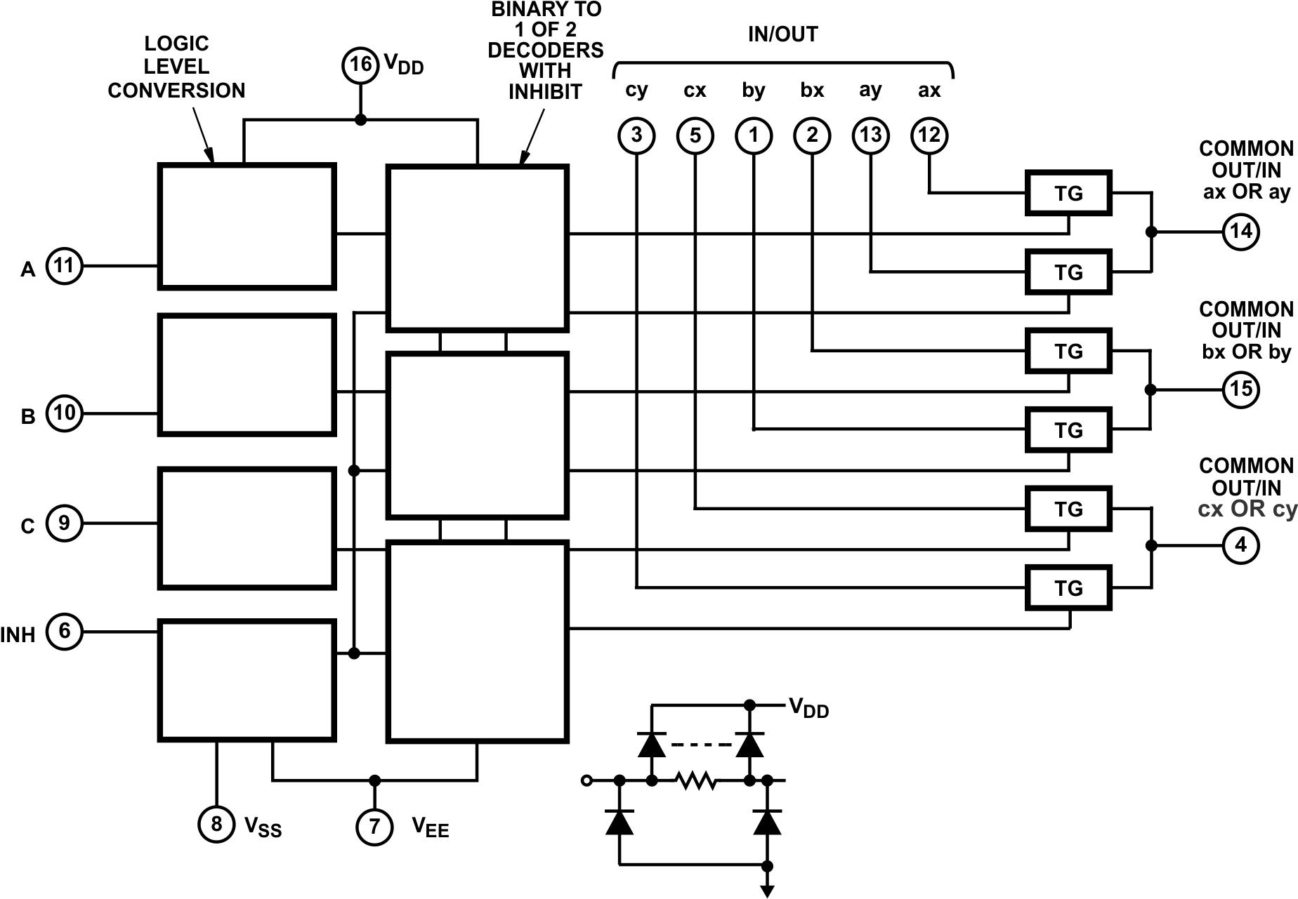
All inputs are protected by standard CMOS protection network.
Figure 8-3 Functional Block Diagram, CD4053B