ZHCSMR2B December 2020 – December 2021 BQ76942
PRODUCTION DATA
- 1 特性
- 2 应用
- 3 说明
- 4 Revision History
- 5 Device Comparison Table
- 6 Pin Configuration and Functions
-
7 Specifications
- 7.1 Absolute Maximum Ratings
- 7.2 ESD Ratings
- 7.3 Recommended Operating Conditions
- 7.4 Thermal Information BQ76942
- 7.5 Supply Current
- 7.6 Digital I/O
- 7.7 LD Pin
- 7.8 Precharge (PCHG) and Predischarge (PDSG) FET Drive
- 7.9 FUSE Pin Functionality
- 7.10 REG18 LDO
- 7.11 REG0 Pre-regulator
- 7.12 REG1 LDO
- 7.13 REG2 LDO
- 7.14 Voltage References
- 7.15 Coulomb Counter
- 7.16 Coulomb Counter Digital Filter (CC1)
- 7.17 Current Measurement Digital Filter (CC2)
- 7.18 Current Wake Detector
- 7.19 Analog-to-Digital Converter
- 7.20 Cell Balancing
- 7.21 Cell Open Wire Detector
- 7.22 Internal Temperature Sensor
- 7.23 Thermistor Measurement
- 7.24 Internal Oscillators
- 7.25 High-Side NFET Drivers
- 7.26 Comparator-Based Protection Subsystem
- 7.27 Timing Requirements – I2C Interface, 100kHz Mode
- 7.28 Timing Requirements – I2C Interface, 400kHz Mode
- 7.29 Timing Requirements – HDQ Interface
- 7.30 Timing Requirements – SPI Interface
- 7.31 Interface Timing Diagrams
- 7.32 Typical Characteristics
- 8 Device Description
- 9 Device Configuration
-
10Measurement Subsystem
- 10.1 Voltage Measurement
- 10.2 General Purpose ADCIN Functionality
- 10.3 Coulomb Counter and Digital Filters
- 10.4 Synchronized Voltage and Current Measurement
- 10.5 Internal Temperature Measurement
- 10.6 Thermistor Temperature Measurement
- 10.7 Factory Trim of Voltage ADC
- 10.8 Voltage Calibration (ADC Measurements)
- 10.9 Voltage Calibration (COV and CUV Protections)
- 10.10 Current Calibration
- 10.11 Temperature Calibration
- 11Primary and Secondary Protection Subsystems
-
12Device Hardware Features
- 12.1 Voltage References
- 12.2 ADC Multiplexer
- 12.3 LDOs
- 12.4 Standalone Versus Host Interface
- 12.5 Multifunction Pin Controls
- 12.6 RST_SHUT Pin Operation
- 12.7 CFETOFF, DFETOFF, BOTHOFF Pin Functionality
- 12.8 ALERT Pin Operation
- 12.9 DDSG and DCHG Pin Operation
- 12.10 Fuse Drive
- 12.11 Cell Open Wire
- 12.12 Low Frequency Oscillator
- 12.13 High Frequency Oscillator
- 13Device Functional Modes
- 14Serial Communications Interface
- 15Cell Balancing
- 16Application and Implementation
- 17Power Supply Requirements
- 18Layout
- 19Device and Documentation Support
- 20Mechanical, Packaging, Orderable Information
10.6 Thermistor Temperature Measurement
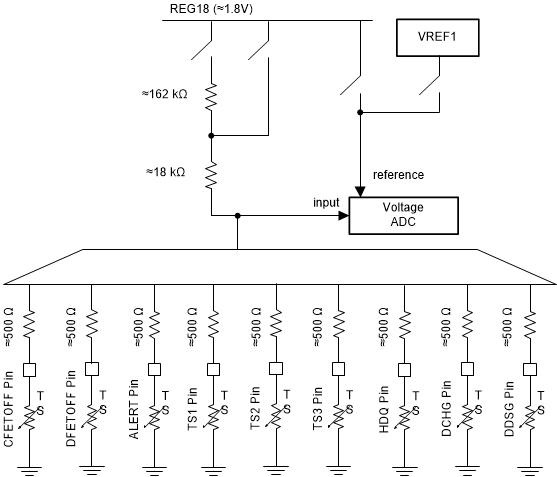
The BQ76942 device includes an on-chip temperature measurement and can support up to nine external thermistors on multifunction pins (TS1, TS2, TS3, CFETOFF, DFETOFF, ALERT, HDQ, DCHG, and DDSG). The device includes an internal pullup resistor to bias a thermistor during measurement.
The internal pullup resistor has two options that can set the pullup resistor to either 18-kΩ or 180-kΩ (or none at all). The 18-kΩ option is intended for use with thermistors such as the Semitec 103-AT, which has 10-kΩ resistance at room temperature. The 180-kΩ option is intended for use with higher resistance thermistors such as the Semitec 204AP-2, which has 200-kΩ resistance at room temperature. The resistor values are measured during factory production and stored within the device for use during temperature calculation. The individual pin configuration registers determine which pin is used for a thermistor measurement, what value of pullup resistor is used, as well as whether the thermistor measurement is used for a cell or FET temperature reading.
 Figure 10-3 External Thermistor Biasing
To provide a high precision temperature result, the device uses the same 1.8 V LDO voltage for the ADC reference as is used for biasing the thermistor pullup resistor, thereby implementing a ratiometric measurement that removes the error contribution from the LDO voltage level. The device processes the digitized thermistor voltage to calculate the temperature based on multiorder polynomials, which can be programmed by the user based on the specific thermistor selected.