ZHCSMY8B September 2020 – January 2022 BQ769142
PRODUCTION DATA
- 1 特性
- 2 应用
- 3 说明
- 4 Revision History
- 5 Device Comparison Table
- 6 Pin Configuration and Functions
-
7 Specifications
- 7.1 Absolute Maximum Ratings
- 7.2 ESD Ratings
- 7.3 Recommended Operating Conditions
- 7.4 Thermal Information BQ769142
- 7.5 Supply Current
- 7.6 Digital I/O
- 7.7 LD Pin
- 7.8 Precharge (PCHG) and Predischarge (PDSG) FET Drive
- 7.9 FUSE Pin Functionality
- 7.10 REG18 LDO
- 7.11 REG0 Pre-regulator
- 7.12 REG1 LDO
- 7.13 REG2 LDO
- 7.14 Voltage References
- 7.15 Coulomb Counter
- 7.16 Coulomb Counter Digital Filter (CC1)
- 7.17 Current Measurement Digital Filter (CC2)
- 7.18 Current Wake Detector
- 7.19 Analog-to-Digital Converter
- 7.20 Cell Balancing
- 7.21 Cell Open Wire Detector
- 7.22 Internal Temperature Sensor
- 7.23 Thermistor Measurement
- 7.24 Internal Oscillators
- 7.25 High-side NFET Drivers
- 7.26 Comparator-Based Protection Subsystem
- 7.27 Timing Requirements - I2C Interface, 100kHz Mode
- 7.28 Timing Requirements - I2C Interface, 400kHz Mode
- 7.29 Timing Requirements - HDQ Interface
- 7.30 Timing Requirements - SPI Interface
- 7.31 Interface Timing Diagrams
- 7.32 Typical Characteristics
- 8 Device Description
- 9 Device Configuration
-
10Measurement Subsystem
- 10.1 Voltage Measurement
- 10.2 General Purpose ADCIN Functionality
- 10.3 Coulomb Counter and Digital Filters
- 10.4 Synchronized Voltage and Current Measurement
- 10.5 Internal Temperature Measurement
- 10.6 Thermistor Temperature Measurement
- 10.7 Factory Trim of Voltage ADC
- 10.8 Voltage Calibration (ADC Measurements)
- 10.9 Voltage Calibration (COV and CUV Protections)
- 10.10 Current Calibration
- 10.11 Temperature Calibration
- 11Primary and Secondary Protection Subsystems
-
12Device
Hardware Features
- 12.1 Voltage References
- 12.2 ADC Multiplexer
- 12.3 LDOs
- 12.4 Standalone Versus Host Interface
- 12.5 Multifunction Pin Controls
- 12.6 RST_SHUT Pin Operation
- 12.7 CFETOFF, DFETOFF, and BOTHOFF Pin Functionality
- 12.8 ALERT Pin Operation
- 12.9 DDSG and DCHG Pin Operation
- 12.10 Fuse Drive
- 12.11 Cell Open Wire
- 12.12 Low Frequency Oscillator
- 12.13 High Frequency Oscillator
- 13Device Functional Modes
- 14Serial Communications Interface
- 15Cell Balancing
- 16Application and Implementation
- 17Power Supply Requirements
- 18Layout
- 19Device and Documentation Support
- 20Mechanical, Packaging, Orderable Information
12.10 Fuse Drive
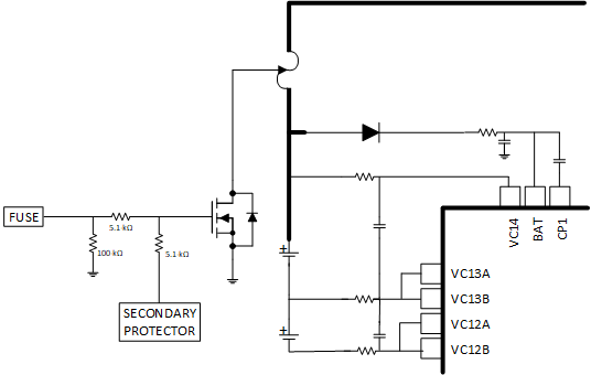
The FUSE pin on the BQ769142 device can be used to blow a chemical fuse in the presence of a Permanent Fail (PF), as well as to determine if an external secondary protector in the system has detected a fault and is attempting to blow the fuse itself. The pin can drive the gate of an NFET, which can be combined with the drive from an external secondary protector, as shown in Figure 12-1. When the FUSE pin is not asserted by the BQ769142 device, it remains in a high-impedance state and detects a voltage applied at the pin by a secondary protector. The device can be configured to generate a PF if it detects a high signal at the FUSE pin.
The device can be configured to blow the fuse when a PF occurs. In this case, the device will only attempt to blow the fuse if the stack voltage is above a programmed threshold, based on a system configuration with the fuse placed between the top of stack and the high-side protection FETs. If instead the fuse is placed between the FETs and the PACK+ connector, then the device bases its decision on the PACK pin voltage (based on configuration setting). This voltage threshold check may be disregarded under certain special cases, as described in the BQ769142 Technical Reference Manual .
 Figure 12-1 FUSE Pin Operation