SLUSFR7 August 2025 BQ24810
PRODUCTION DATA
- 1
- 1 Features
- 2 Applications
- 3 Description
- 4 Pin Configuration and Functions
- 5 Specifications
-
6 Detailed Description
- 6.1 Overview
- 6.2 Functional Block Diagram
- 6.3
Feature Description
- 6.3.1 Device Power Up
- 6.3.2 System Power Selection
- 6.3.3 Current and Power Monitor
- 6.3.4 Processor Hot Indication for CPU Throttling
- 6.3.5 Input Current Dynamic Power Management
- 6.3.6 Two-Level Adapter Current Limit (Peak Power Mode)
- 6.3.7 EMI Switching Frequency Adjust
- 6.3.8 Device Protections Features
- 6.4 Device Functional Modes
- 6.5 Programming
- 6.6
Register Maps
- 6.6.1 Battery-Charger Commands
- 6.6.2 Setting Charger Options
- 6.6.3 ChargeOption1 Register
- 6.6.4 ChargeOption2 Register
- 6.6.5 ChargeOption3 Register
- 6.6.6 ChargeOption4 Register
- 6.6.7 ProchotOption0 Register
- 6.6.8 ProchotOption1 Register
- 6.6.9 ProchotStatus Register
- 6.6.10 Charge Current Register
- 6.6.11 Charge Voltage Register
- 6.6.12 Discharge Current Register
- 6.6.13 Minimum System Voltage Register
- 6.6.14 Input Current Register
- 6.6.15 Register Exceptions
-
7 Application and Implementation
- 7.1 Application Information
- 7.2
Typical Applications
- 7.2.1
Typical System Schematic
- 7.2.1.1 Design Requirements
- 7.2.1.2
Detailed Design Procedure
- 7.2.1.2.1 Adapter Current Sense Filter
- 7.2.1.2.2 Negative Output Voltage Protection
- 7.2.1.2.3 Reverse Input Voltage Protection
- 7.2.1.2.4 Reduce Battery Quiescent Current
- 7.2.1.2.5 CIN Capacitance
- 7.2.1.2.6 L1 Inductor Selection
- 7.2.1.2.7 CBATT Capacitance
- 7.2.1.2.8 Buck Charging Internal Compensation
- 7.2.1.2.9 CSYS Capacitance
- 7.2.1.2.10 Battery Only Boost Internal Compensation
- 7.2.1.2.11 Power MOSFETs Selection
- 7.2.1.2.12 Input Filter Design
- 7.2.1.3 Application Curves
- 7.2.2 Migration from Previous Devices (Does Not Support Battery Only Boost)
- 7.2.1
Typical System Schematic
- 7.3 Power Supply Recommendations
- 7.4 Layout
- 8 Device and Documentation Support
- 9 Revision History
- 10Mechanical, Packaging, and Orderable Information
7.2.1.2.8 Buck Charging Internal Compensation
The synchronous buck PWM converter uses a fixed frequency voltage control scheme and internal type III compensation network. The LC output filter gives a characteristic resonant frequency:
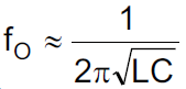
The resonant frequency, fo, is used to determine the compensation to ensure there is sufficient phase margin for the target bandwidth. The LC output filter should be selected to give a resonant frequency of 10- to 20-kHz nominal for the best performance. Suggested component values for different ChargeCurrent() REG0x14 settings are shown in Table 7-2 to Table 7-3 for the available switching frequencies of 300 - 800 kHz. Note that these tables are generated based on the charging configuration, so the Output Capacitor is the capacitance at the battery connection, close to the SRN node of the battery charging sense resistor. The procedure for generating these tables is to first select the inductor value to have a ripple current that is in the range of 20 - 40% of the target charge current. Once the inductor value has been calculated, the output capacitance is chosen to have an output stage resonant frequency between 10- to 20-kHz.
| CHARGE CURRENT | 2A | 3A | 4A | 6A | 8A |
|---|---|---|---|---|---|
| L1 (µH) | 6.8 or 8.2 | 5.6 or 6.8 | 3.3 or 4.7 | 3.3 | 2.2 |
| CBATT (µF) (Effective after derating) | 20 | 20 | 20 | 30 | 40 |
| CHARGE CURRENT | 3A | 4A | 5A | 6A | 8A |
|---|---|---|---|---|---|
| L1 (µH) | 10 | 6.8 or 8.2 | 6.8 | 5.6 | 4.7 |
| CBATT (µF) (Effective after derating) | 15 | 20 | 20 | 20 | 20 |
Ceramic capacitors show a DC-bias effect. This effect reduces the effective capacitance when a DC-bias voltage is applied across a ceramic capacitor, as on the output capacitor of a charger. The effect may lead to a significant capacitance drop, especially for high output voltages and small capacitor packages. See the manufacturer's data sheet about the performance with a DC bias voltage applied. It may be necessary to choose a higher voltage rating or nominal capacitance value to get the required value at the operating point.