SLUS805C April 2008 – August 2015
PRODUCTION DATA.
- 1 Features
- 2 Applications
- 3 Description
- 4 Revision History
- 5 Pin Configuration and Functions
- 6 Specifications
- 7 Detailed Description
- 8 Application and Implementation
- 9 Power Supply Recommendations
- 10Layout
- 11Device and Documentation Support
- 12Mechanical, Packaging, and Orderable Information
8 Application and Implementation
NOTE
Information in the following applications sections is not part of the TI component specification, and TI does not warrant its accuracy or completeness. TI’s customers are responsible for determining suitability of components for their purposes. Customers should validate and test their design implementation to confirm system functionality.
8.1 Application Information
The bq2438x device protects against overvoltage and battery overvoltage events that occur due to faulty adapter or incorrect input sources. If either of these faults occur, the bq2438x device isolates the downstream devices from the input source and alerts the host controller with the FAULT open-drain output.
8.2 Typical Application
 Figure 10. Typical Application Circuit
8.2.1 Design Requirements
For this design example, use the parameters shown in Table 1.
Table 1. Design Parameters
| PARAMETER | VALUE |
|---|---|
| Voltage | 5 V |
| Current | < 1.5 A |
8.2.2 Detailed Design Procedure
8.2.2.1 Selection of R(BAT)
It is strongly recommended that the battery not be tied directly to the VBAT pin of the device, as under some failure modes of the device, the voltage at the IN pin may appear on the VBAT pin. This voltage can be as high as 30 V, and applying 30 V to the battery may cause failure of the device and can be hazardous. Connecting the VBAT pin through R(BAT) prevents a large current from flowing into the battery in the event of failure of the device. For safety, R(BAT) must have a high value. The problem with a large R(BAT) is that the voltage drop across this resistor because of the VBAT bias current, I(VBAT), causes an error in the BVOVP threshold. This error is over and above the tolerance on the nominal 4.35-V BVOVP threshold.
Choosing R(BAT) in the range from 100 kΩ to 470 kΩ is a good compromise. If the device fails with R(BAT) equal to 100 kΩ, the maximum current flowing into the battery would be (30 V – 3 V) ÷ 100 kΩ = 246 μA, which is low enough to be absorbed by the bias currents of the system components. R(BAT) equal to 100 kΩ results in a worst-case voltage drop of R(BAT) × I(VBAT) = 1 mV. This is negligible compared to the internal tolerance of 50 mV on the BVOVP threshold.
If the Bat-OVP function is not required, the VBAT pin must be connected to VSS.
8.2.2.2 Selection of R(CE)
The CE pin can be used to enable and disable the device. If host control is not required, the CE pin can be tied to ground or left unconnected, permanently enabling the device.
In applications where external control is required, the CE pin can be controlled by a host processor. As with the VBAT pin (see previous discussion), the CE pin must be connected to the host GPIO pin through as large a resistor as possible. The limitation on the resistor value is that the minimum VOH of the host GPIO pin less the drop across the resistor must be greater than VIH of the bq2438x CE pin. The drop across the resistor is given by R(CE) × IIH.
8.2.2.3 Selection of Input and Output Bypass Capacitors
The input capacitor CIN in Figure 10 is for decoupling and serves an important purpose. Whenever there is a step change downwards in the system load current, the inductance of the input cable causes the input voltage to spike up. CIN prevents the input voltage from overshooting to dangerous levels. It is recommended that a ceramic capacitor of at least 1 μF be used at the input of the device. It must be located in close proximity to the IN pin.
COUT in Figure 10 is also important. During an overvoltage transient, this capacitance limits the output overshoot until the power FET is turned off by the overvoltage protection circuitry. COUT must be a ceramic capacitor of at least 1 μF, located close to the OUT pin. COUT also serves as the input decoupling capacitor for the charging circuit downstream of the protection device.
8.2.3 Application Curves
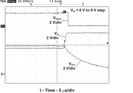
 Figure 13. OVP Response for Input Step (bq24380)
 Figure 15. Recovery from OVP (bq24380)
 Figure 17. Soft-Stop During OCP Event (bq24380)
 Figure 12. OVP at Power-On
 Figure 14. Slow Input Ramp into OVP Event (bq24380)
 Figure 16. Power Up into Short Circuit
 Figure 18. Battery OVP Event (bq24380)
