ZHCSGY5A October   2017  – December 2017

PRODUCTION DATA.  

  1. 特性
  2. 应用范围
  3. 说明
    1.     典型应用电路
  4. 修订历史记录
  5. 说明 (续)
  6. Device Comparison Table
  7. Pin Configuration and Functions
    1.     Pin Functions
    2. 7.1 EN1/EN2 Settings
  8. Specifications
    1. 8.1 Absolute Maximum Ratings
    2. 8.2 ESD Ratings
    3. 8.3 Recommended Operating Conditions
    4. 8.4 Thermal Information
    5. 8.5 Dissipation Ratings
    6. 8.6 Electrical Characteristics
    7. 8.7 Typical Characteristics
  9. Detailed Description
    1. 9.1 Overview
    2. 9.2 Functional Block Diagram
    3. 9.3 Feature Description
      1. 9.3.1 Undervoltage Lockout (UVLO)
      2. 9.3.2 Power On
      3. 9.3.3 Overvoltage Protection (OVP)
      4. 9.3.4 Dynamic Power-Path Management
        1. 9.3.4.1 Input Source Connected (ADAPTER or USB)
          1. 9.3.4.1.1 Input DPM Mode (VIN-DPM)
          2. 9.3.4.1.2 DPPM Mode
          3. 9.3.4.1.3 Battery Supplement Mode
        2. 9.3.4.2 Input Source Not Connected
      5. 9.3.5 Battery Charging
        1. 9.3.5.1 Charge Current Translator
        2. 9.3.5.2 Battery Detection and Recharge
        3. 9.3.5.3 Battery Disconnect (SYSOFF Input, bq24076, bq24078)
        4. 9.3.5.4 Dynamic Charge Timers (TMR Input)
        5. 9.3.5.5 Status Indicators (PGOOD, CHG)
        6. 9.3.5.6 Thermal Regulation and Thermal Shutdown
      6. 9.3.6 Battery Pack Temperature Monitoring
    4. 9.4 Device Functional Modes
      1. 9.4.1 Sleep Mode
      2. 9.4.2 Explanation of Deglitch Times and Comparator Hysteresis
  10. 10Application and Implementation
    1. 10.1 Application Information
    2. 10.2 Typical Application
      1. 10.2.1 Design Requirements
      2. 10.2.2 Detailed Design Procedure
        1. 10.2.2.1 bq2407x Charger Design Example
          1. 10.2.2.1.1 System ON/OFF (SYSOFF) (bq24076 or bq24078 only)
        2. 10.2.2.2 Calculations
          1. 10.2.2.2.1 Program the Fast Charge Current (ISET):
          2. 10.2.2.2.2 Program the Input Current Limit (ILIM)
          3. 10.2.2.2.3 Program 6.25-hour Fast-Charge Safety Timer (TMR)
        3. 10.2.2.3 TS Function
        4. 10.2.2.4 CHG and PGOOD
        5. 10.2.2.5 Selecting IN, OUT, and BAT Pin Capacitors
      3. 10.2.3 Application Curves
  11. 11Power Supply Recommendations
  12. 12Layout
    1. 12.1 Layout Guidelines
    2. 12.2 Layout Example
    3. 12.3 Thermal Considerations
  13. 13器件和文档支持
    1. 13.1 器件支持
      1. 13.1.1 Third-Party Products Disclaimer
    2. 13.2 相关链接
    3. 13.3 接收文档更新通知
    4. 13.4 社区资源
    5. 13.5 商标
    6. 13.6 静电放电警告
    7. 13.7 Glossary
  14. 14机械、封装和可订购信息

封装选项

机械数据 (封装 | 引脚)
散热焊盘机械数据 (封装 | 引脚)
订购信息

Application Curves

bq24076 bq24078 bat_conn_lus810.gif
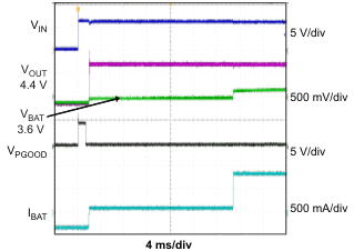
RLOAD = 10 Ω
Figure 27. Adapter Plug-In
Battery Connected
bq24076 bq24078 hot_plug2_lus810.gif
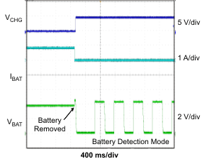
Figure 29. Battery Detection
Battery Removed
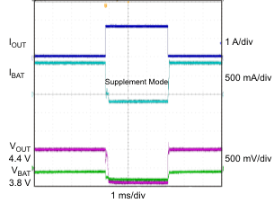
bq24076 bq24078 batt_mode_lus810.gif
RLOAD = 25 Ω to 4.5 Ω
Figure 31. Entering and Exiting Battery Supplement Mode
bq24076 bq24078 on_off_chgr_lus810.gif
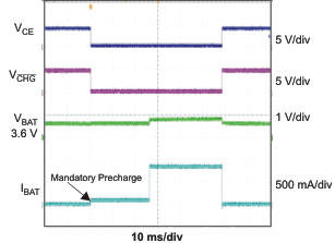
Figure 33. Charger ON/OFF Using CE
bq24076 bq24078 system_of6v_lus810.gif
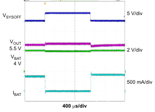
VIN = 6 V
Figure 35. System ON/OFF With Input Connected
bq24076, bq24078
bq24076 bq24078 hot_plug_lus810.gif
Figure 28. Battery Detection
Battery Inserted
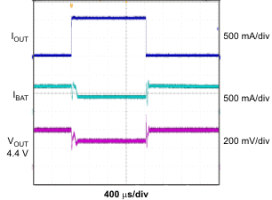
bq24076 bq24078 dppm_mode_lus810.gif
RLOAD = 20 Ω to 9 Ω
Figure 30. Entering and Exiting DPPM Mode
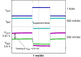
bq24076 bq24078 supp_mode_luscm1.gif
RLOAD = 20 Ω to 4.5 Ω
Figure 32. Entering and Exiting Battery Supplement Mode
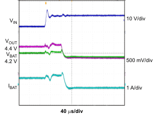
bq24076 bq24078 ovp_fault_lus810.gif
VIN = 6 V to 15 V RLOAD = 10 Ω
Figure 34. OVP Fault
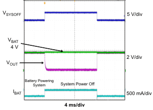
bq24076 bq24078 system_of0v_lus810.gif
VIN = 0 V
Figure 36. System ON/OFF With Input Not Connected
bq24076, bq24078