SPRS658F February 2010 – March 2014 AM1806
PRODUCTION DATA.
- 1 AM1806 ARM Microprocessor
- 2Revision History
-
3Device Overview
- 3.1 Device Characteristics
- 3.2 Device Compatibility
- 3.3 ARM Subsystem
- 3.4 Memory Map Summary
- 3.5 Pin Assignments
- 3.6 Pin Multiplexing Control
- 3.7
Terminal Functions
- 3.7.1 Device Reset and JTAG
- 3.7.2 High-Frequency Oscillator and PLL
- 3.7.3 Real-Time Clock and 32-kHz Oscillator
- 3.7.4 DEEPSLEEP Power Control
- 3.7.5 External Memory Interface A (EMIFA)
- 3.7.6 DDR2/mDDR Memory Controller
- 3.7.7 Serial Peripheral Interface Modules (SPI)
- 3.7.8 Programmable Real-Time Unit (PRU)
- 3.7.9 Enhanced Capture/Auxiliary PWM Modules (eCAP0)
- 3.7.10 Enhanced Pulse Width Modulators (eHRPWM)
- 3.7.11 Boot
- 3.7.12 Universal Asynchronous Receiver/Transmitters (UART0, UART1, UART2)
- 3.7.13 Inter-Integrated Circuit Modules(I2C0, I2C1)
- 3.7.14 Timers
- 3.7.15 Multichannel Audio Serial Ports (McASP)
- 3.7.16 Multichannel Buffered Serial Ports (McBSP)
- 3.7.17 Universal Serial Bus Modules (USB0)
- 3.7.18 Multimedia Card/Secure Digital (MMC/SD)
- 3.7.19 Liquid Crystal Display Controller(LCD)
- 3.7.20 Universal Host-Port Interface (UHPI)
- 3.7.21 Universal Parallel Port (uPP)
- 3.7.22 Video Port Interface (VPIF)
- 3.7.23 General Purpose Input Output
- 3.7.24 Reserved and No Connect
- 3.7.25 Supply and Ground
- 3.8 Unused Pin Configurations
- 4Device Configuration
-
5Specifications
- 5.1 Absolute Maximum Ratings Over Operating Junction Temperature Range (Unless Otherwise Noted)
- 5.2 Handling Ratings
- 5.3 Recommended Operating Conditions
- 5.4 Notes on Recommended Power-On Hours (POH)
- 5.5 Electrical Characteristics Over Recommended Ranges of Supply Voltage and Operating Junction Temperature (Unless Otherwise Noted)
-
6Peripheral Information and Electrical Specifications
- 6.1 Parameter Information
- 6.2 Recommended Clock and Control Signal Transition Behavior
- 6.3 Power Supplies
- 6.4 Reset
- 6.5 Crystal Oscillator or External Clock Input
- 6.6 Clock PLLs
- 6.7 Interrupts
- 6.8 Power and Sleep Controller (PSC)
- 6.9 EDMA
- 6.10 External Memory Interface A (EMIFA)
- 6.11
DDR2/mDDR Memory Controller
- 6.11.1 DDR2/mDDR Memory Controller Electrical Data/Timing
- 6.11.2 DDR2/mDDR Controller Register Description(s)
- 6.11.3
DDR2/mDDR Interface
- 6.11.3.1 DDR2/mDDR Interface Schematic
- 6.11.3.2 Compatible JEDEC DDR2/mDDR Devices
- 6.11.3.3 PCB Stackup
- 6.11.3.4 Placement
- 6.11.3.5 DDR2/mDDR Keep Out Region
- 6.11.3.6 Bulk Bypass Capacitors
- 6.11.3.7 High-Speed Bypass Capacitors
- 6.11.3.8 Net Classes
- 6.11.3.9 DDR2/mDDR Signal Termination
- 6.11.3.10 VREF Routing
- 6.11.3.11 DDR2/mDDR CK and ADDR_CTRL Routing
- 6.11.3.12 MDDR/DDR2 Boundary Scan Limitations
- 6.12 Memory Protection Units
- 6.13 MMC / SD / SDIO (MMCSD0, MMCSD1)
- 6.14 Multichannel Audio Serial Port (McASP)
- 6.15 Multichannel Buffered Serial Port (McBSP)
- 6.16 Serial Peripheral Interface Ports (SPI0, SPI1)
- 6.17 Inter-Integrated Circuit Serial Ports (I2C)
- 6.18 Universal Asynchronous Receiver/Transmitter (UART)
- 6.19 Universal Serial Bus OTG Controller (USB0) [USB2.0 OTG]
- 6.20 LCD Controller (LCDC)
- 6.21 Host-Port Interface (UHPI)
- 6.22 Universal Parallel Port (uPP)
- 6.23 Video Port Interface (VPIF)
- 6.24 Enhanced Capture (eCAP) Peripheral
- 6.25 Enhanced High-Resolution Pulse-Width Modulator (eHRPWM)
- 6.26 Timers
- 6.27 Real Time Clock (RTC)
- 6.28 General-Purpose Input/Output (GPIO)
- 6.29 Programmable Real-Time Unit Subsystem (PRUSS)
- 6.30 Emulation Logic
- 7Device and Documentation Support
- 8Mechanical Packaging and Orderable Information
封装选项
请参考 PDF 数据表获取器件具体的封装图。
机械数据 (封装 | 引脚)
- ZCE|361
- ZWT|361
散热焊盘机械数据 (封装 | 引脚)
订购信息
1 AM1806 ARM Microprocessor
1.1 Features
- 375- and 456-MHz ARM926EJ-S™ RISC MPU
- Enhanced Direct Memory Access Controller 3 (EDMA3):
- 2 Channel Controllers
- 3 Transfer Controllers
- 64 Independent DMA Channels
- 16 Quick DMA Channels
- Programmable Transfer Burst Size
- 1.8-V or 3.3-V LVCMOS I/Os (Except for USB and DDR2 Interfaces)
- Two External Memory Interfaces:
- EMIFA
- NOR (8- or 16-Bit-Wide Data)
- NAND (8- or 16-Bit-Wide Data)
- 16-Bit SDRAM with 128-MB Address Space
- DDR2/Mobile DDR Memory Controller with one of the following:
- 16-Bit DDR2 SDRAM with 256-MB Address Space
- 16-Bit mDDR SDRAM with 256-MB Address Space
- Three Configurable 16550-Type UART Modules:
- With Modem Control Signals
- 16-Byte FIFO
- 16x or 13x Oversampling Option
- LCD Controller
- Two Serial Peripheral Interfaces (SPIs) Each with Multiple Chip Selects
- Two Multimedia Card (MMC)/Secure Digital (SD) Card Interfaces with Secure Data I/O (SDIO) Interfaces
- Two Master and Slave Inter-Integrated Circuits
(I2C Bus™) - One Host-Port Interface (HPI) with 16-Bit-Wide Muxed Address and Data Bus For High Bandwidth
- Programmable Real-Time Unit Subsystem (PRUSS)
- Two Independent Programmable Real-Time Unit (PRU) Cores
- 32-Bit Load-Store RISC Architecture
- 4KB of Instruction RAM per Core
- 512 Bytes of Data RAM per Core
- PRUSS can be Disabled via Software to Save Power
- Register 30 of Each PRU is Exported from the Subsystem in Addition to the Normal R31 Output of the PRU Cores.
- Standard Power-Management Mechanism
- Clock Gating
- Entire Subsystem Under a Single PSC Clock Gating Domain
- Dedicated Interrupt Controller
- Dedicated Switched Central Resource
- USB 2.0 OTG Port with Integrated PHY (USB0)
- USB 2.0 High- and Full-Speed Client
- USB 2.0 High-, Full-, and Low-Speed Host
- End Point 0 (Control)
- End Points 1,2,3,4 (Control, Bulk, Interrupt or ISOC) RX and TX
- One Multichannel Audio Serial Port (McASP):
- Transmit and Receive Clocks
- Two Clock Zones and 16 Serial Data Pins
- Supports TDM, I2S, and Similar Formats
- DIT-Capable
- FIFO Buffers for Transmit and Receive
- Two Multichannel Buffered Serial Ports (McBSPs):
- Transmit and Receive Clocks
- Supports TDM, I2S, and Similar Formats
- AC97 Audio Codec Interface
- Telecom Interfaces (ST-Bus, H100)
- 128-Channel TDM
- FIFO Buffers for Transmit and Receive
- Video Port Interface (VPIF):
- Two 8-Bit SD (BT.656), Single 16-Bit or Single Raw (8-, 10-, and 12-Bit) Video Capture Channels
- Two 8-Bit SD (BT.656), Single 16-Bit Video Display Channels
- Universal Parallel Port (uPP):
- High-Speed Parallel Interface to FPGAs and Data Converters
- Data Width on Both Channels is 8- to 16-Bit Inclusive
- Single-Data Rate or Dual-Data Rate Transfers
- Supports Multiple Interfaces with START, ENABLE, and WAIT Controls
- Real-Time Clock (RTC) with 32-kHz Oscillator and Separate Power Rail
- Three 64-Bit General-Purpose Timers (Each Configurable as Two 32-Bit Timers)
- One 64-Bit General-Purpose or Watchdog Timer (Configurable as Two 32-Bit General-Purpose Timers)
- Two Enhanced High-Resolution Pulse Width Modulators (eHRPWMs):
- Dedicated 16-Bit Time-Base Counter with Period and Frequency Control
- 6 Single-Edge Outputs, 6 Dual-Edge Symmetric Outputs, or 3 Dual-Edge Asymmetric Outputs
- Dead-Band Generation
- PWM Chopping by High-Frequency Carrier
- Trip Zone Input
- Three 32-Bit Enhanced Capture (eCAP) Modules:
- Configurable as 3 Capture Inputs or 3 Auxiliary Pulse Width Modulator (APWM) Outputs
- Single-Shot Capture of up to Four Event Time-Stamps
- 361-Ball Pb-Free Plastic Ball Grid Array (PBGA) [ZCE Suffix], 0.65-mm Ball Pitch
- 361-Ball Pb-Free PBGA [ZWT Suffix], 0.80-mm Ball Pitch
- Commercial or Extended Temperature
1.2 Applications
- Gaming
- Medical, Healthcare, Fitness
- Printers
- ePOS
- Data Concentrators
- Building Automation
- Set Top Box
- Industrial Automation
1.3 Description
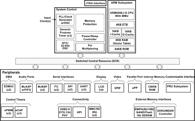
The AM1806 ARM Microprocessor is a low-power applications processor based on ARM926EJ-S.
The device enables original-equipment manufacturers (OEMs) and original-design manufacturers (ODMs) to quickly bring to market devices featuring robust operating systems support, rich user interfaces, and high processing performance life through the maximum flexibility of a fully integrated mixed processor solution.
The ARM926EJ-S is a 32-bit RISC processor core that performs 32-bit or 16-bit instructions and processes 32-bit, 16-bit, or 8-bit data. The core uses pipelining so that all parts of the processor and memory system can operate continuously.
The ARM core has a coprocessor 15 (CP15), protection module, and data and program memory management units (MMUs) with table look-aside buffers. The ARM core processor has separate 16-KB instruction and 16-KB data caches. Both are four-way associative with virtual index virtual tag (VIVT). The ARM core also has 8KB of RAM (Vector Table) and 64KB of ROM.
The peripheral set includes: one USB2.0 OTG interface; two inter-integrated circuit (I2C Bus) interfaces; one multichannel audio serial port (McASP) with 16 serializers and FIFO buffers; two multichannel buffered serial ports (McBSPs) with FIFO buffers; two serial peripheral interfaces (SPIs) with multiple chip selects; four 64-bit general-purpose timers each configurable (one configurable as watchdog); a configurable 16-bit host-port interface (HPI); up to 9 banks of general-purpose input/output (GPIO) pins, with each bank containing 16 pins with programmable interrupt and event generation modes, multiplexed with other peripherals; three UART interfaces (each with RTS and CTS); two enhanced high-resolution pulse width modulator (eHRPWM) peripherals; three 32-bit enhanced capture (eCAP) module peripherals which can be configured as 3 capture inputs or 3 auxiliary pulse width modulator (APWM) outputs; two external memory interfaces; an asynchronous and SDRAM external memory interface (EMIFA) for slower memories or peripherals; and a higher speed DDR2/Mobile DDR controller.
The universal parallel port (uPP) provides a high-speed interface to many types of data converters, FPGAs or other parallel devices. The uPP supports programmable data widths between 8- to 16-bits on both channels. Single-data rate and double-data rate transfers are supported as well as START, ENABLE, and WAIT signals to provide control for a variety of data converters.
A video port interface (VPIF) is included providing a flexible video I/O port.
The rich peripheral set provides the ability to control external peripheral devices and communicate with external processors. For details on each of the peripherals, see the related sections in this document and the associated peripheral reference guides.
The device has a complete set of development tools for the ARM processor. These tools include C compilers, and scheduling, and a Windows® debugger interface for visibility into source code execution.
Device Information
| PART NUMBER | PACKAGE | BODY SIZE |
|---|---|---|
| AM1806ZCE | NFBGA (361) | 13,00 mm x 13,00 mm |
| AM1806ZWT | NFBGA (361) | 16,00 mm x 16,00 mm |
1.4 Functional Block Diagram
Figure 1-1 shows the functional block diagram of the device.