ZHCSMK3B November 2020 – November 2021 ADS131B04-Q1
PRODUCTION DATA
- 1 特性
- 2 应用
- 3 说明
- 4 Revision History
- 5 Pin Configuration and Functions
- 6 Specifications
- 7 Parameter Measurement Information
-
8 Detailed Description
- 8.1 Overview
- 8.2 Functional Block Diagram
- 8.3 Feature Description
- 8.4 Device Functional Modes
- 8.5
Programming
- 8.5.1
Serial Interface
- 8.5.1.1 Chip Select (CS)
- 8.5.1.2 Serial Data Clock (SCLK)
- 8.5.1.3 Serial Data Input (DIN)
- 8.5.1.4 Serial Data Output (DOUT)
- 8.5.1.5 Data Ready (DRDY)
- 8.5.1.6 SPI Communication Frames
- 8.5.1.7 SPI Communication Words
- 8.5.1.8 Short SPI Frames
- 8.5.1.9 Communication Cyclic Redundancy Check (CRC)
- 8.5.1.10 SPI Timeout
- 8.5.2 ADC Conversion Data Format
- 8.5.3 Commands
- 8.5.4 Collecting Data for the First Time or After a Pause in Data Collection
- 8.5.1
Serial Interface
- 8.6 Register Map
- 9 Application and Implementation
- 10Power Supply Recommendations
- 11Layout
- 12Device and Documentation Support
- 13Mechanical, Packaging, and Orderable Information
8.5.1.6 SPI Communication Frames
SPI communication on the ADS131B04-Q1 is performed in frames. Each SPI communication frame consists of several words. The word size is configurable as either 16 bits, 24 bits, or 32 bits by programming the WLENGTH[1:0] bits in the MODE register.
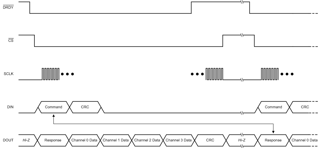
The interface is full duplex, meaning that the interface is capable of transmitting data on DOUT while simultaneously receiving data on DIN. The input frame that the host sends on DIN always begins with a command. The first word on the output frame that the device transmits on DOUT always begins with the response to the command that was written on the previous input frame. The number of words in a command depends on the command provided. For most commands, there are six words in a frame. On DIN, the host provides the command, the command CRC if input CRC is enabled or a word of zeros if input CRC is disabled, and four additional words of zeros. Simultaneously on DOUT, the device outputs the response from the previous frame command, four words of ADC data representing the four ADC channels, and a CRC word. Figure 8-14 shows a typical command frame structure.
 Figure 8-14 Typical
Communication Frame
Figure 8-14 Typical
Communication FrameThere are some commands that require more or less than six words. In the case of a read register (RREG) command where more than a single register is read, the response to the command contains the acknowledgment of the command followed by the register contents requested, which may require a shorter or longer frame depending on how many registers are read. See the RREG command section for more details on the RREG command.
In the case of a write register (WREG) command where more than a single register is written, the frame extends to accommodate the additional data. See the WREG command section for more details on the WREG command.
See the Section 8.5.3 section for a list of all valid commands and their corresponding responses on the ADS131B04-Q1.
Under special circumstances, a data frame can be shortened by the host. See the Section 8.5.1.8 section for more information about artificially shortening communication frames.