ZHCSQZ9A March 2022 – October 2022 ADS117L11
PRODUCTION DATA
- 1 特性
- 2 应用
- 3 说明
- 4 Revision History
- 5 Pin Configuration and Functions
-
6 Specifications
- 6.1 Absolute Maximum Ratings
- 6.2 ESD Ratings
- 6.3 Recommended Operating Conditions
- 6.4 Thermal Information
- 6.5 Electrical Characteristics
- 6.6 Timing Requirements (1.65 V ≤ IOVDD ≤ 2 V)
- 6.7 Switching Characteristics (1.65 V ≤ IOVDD ≤ 2 V)
- 6.8 Timing Requirements (2 V < IOVDD ≤ 5.5 V)
- 6.9 Switching Characteristics (2 V < IOVDD ≤ 5.5 V)
- 6.10 Timing Diagrams
- 6.11 Typical Characteristics
- 7 Parameter Measurement Information
-
8 Detailed Description
- 8.1 Overview
- 8.2 Functional Block Diagram
- 8.3 Feature Description
- 8.4 Device Functional Modes
- 8.5 Programming
- 8.6
Registers
- 8.6.1 DEV_ID Register (Address = 0h) [reset = 01h]
- 8.6.2 REV_ID Register (Address = 1h) [reset = xxh]
- 8.6.3 STATUS Register (Address = 2h) [reset = x1100xxxb]
- 8.6.4 CONTROL Register (Address = 3h) [reset = 00h]
- 8.6.5 MUX Register (Address = 4h) [reset = 00h]
- 8.6.6 CONFIG1 Register (Address = 5h) [reset = 00h]
- 8.6.7 CONFIG2 Register (Address = 6h) [reset = 00h]
- 8.6.8 CONFIG3 Register (Address = 7h) [reset = 00h]
- 8.6.9 CONFIG4 Register (Address = 8h) [reset = 08h]
- 8.6.10 OFFSET2, OFFSET1, OFFSET0 Registers (Addresses = 9h, Ah, Bh) [reset = 00h, 00h, 00h]
- 8.6.11 GAIN2, GAIN1, GAIN0 Registers (Addresses = Ch, Dh, Eh) [reset = 40h, 00h, 00h]
- 8.6.12 CRC Register (Address = Fh) [reset = 00h]
- 9 Application and Implementation
- 10Device and Documentation Support
- 11Mechanical, Packaging, and Orderable Information
8.3.5.2.1 Sinc4 Filter
The sinc4 filter averages and decimates the high-speed modulator data to yield data rates from 1066.6 kSPS to 3.125 kSPS in high-speed mode, and data rates from 133.333 kSPS to 0.390625 kSPS in low-speed mode. Increasing the OSR value decreases the data rate and simultaneously reduces signal bandwidth and total noise resulting from increased decimation and data averaging. Table 8-4 lists the sinc4 filter characteristics.
| OSR | DATA RATE (kSPS) | –3-dB FREQUENCY (kHz) | LATENCY TIME (µs)(1) |
|---|---|---|---|
| HIGH-SPEED MODE (fCLK = 25.6 MHz) | |||
| 12 | 1066.666 | 242.666 | 4.38 |
| 16 | 800 | 182 | 5.63 |
| 24 | 533.333 | 121.333 | 8.13 |
| 32 | 400 | 91.0 | 10.63 |
| 64 | 200 | 45.5 | 20.63 |
| 128 | 100 | 22.75 | 40.63 |
| 256 | 50 | 11.375 | 80.63 |
| 512 | 25 | 5.687 | 160.63 |
| 1024 | 12.5 | 2.844 | 320.63 |
| 2048 | 6.25 | 1.422 | 640.63 |
| 4096 | 3.125 | 0.711 | 1280.63 |
| LOW-SPEED MODE (fCLK = 3.2 MHz) | |||
| 12 | 133.333 | 30.333 | 35.04 |
| 16 | 100 | 22.75 | 45.04 |
| 24 | 66.666 | 15.166 | 65.04 |
| 32 | 50 | 11.375 | 85.04 |
| 64 | 25 | 5.687 | 165.04 |
| 128 | 12.5 | 2.844 | 325.04 |
| 256 | 6.25 | 1.422 | 645.04 |
| 512 | 3.125 | 0.711 | 1285.04 |
| 1024 | 1.5625 | 0.355 | 2565.04 |
| 2048 | 0.78125 | 0.177 | 5125.04 |
| 4096 | 0.390625 | 0.089 | 10245.04 |
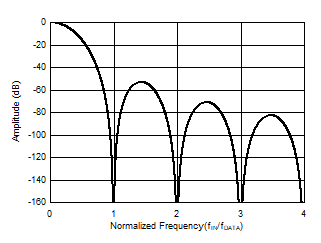
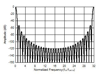
Figure 8-14 and Figure 8-15 show the sinc4 filter frequency response at OSR = 32. The frequency response consists of a series of response nulls occurring at discrete frequencies. The null frequencies occur at multiples of fDATA. At the null frequencies, the filter has zero gain. A folded image of the overall frequency response appears at multiples of fMOD, as illustrated in the fMOD frequency plot of Figure 8-15. No attenuation is provided by the filter at input frequencies near n · fMOD (n = 1, 2, 3, and so on), and if present, alias into the pass band.
 Figure 8-14 Sinc4 Frequency
Response
Figure 8-14 Sinc4 Frequency
Response(OSR = 32)
 Figure 8-15 Sinc4 Frequency Response
to fMOD (OSR = 32)