ZHCSQN6 May   2022 ADC3644

PRODUCTION DATA  

  1. 特性
  2. 应用
  3. 说明
  4. Revision History
  5. Pin Configuration and Functions
  6. Specifications
    1. 6.1 Absolute Maximum Ratings
    2. 6.2 ESD Ratings
    3. 6.3 Recommended Operating Conditions
    4. 6.4 Thermal Information
    5. 6.5 Electrical Characteristics - Power Consumption
    6. 6.6 Electrical Characteristics - DC Specifications
    7. 6.7 Electrical Characteristics - AC Specifications
    8. 6.8 Timing Requirements
    9. 6.9 Typical Characteristics
  7. Parameter Measurement Information
  8. Detailed Description
    1. 8.1 Overview
    2. 8.2 Functional Block Diagram
    3. 8.3 Feature Description
      1. 8.3.1 Analog Input
        1. 8.3.1.1 Analog Input Bandwidth
        2. 8.3.1.2 Analog Front End Design
          1. 8.3.1.2.1 Sampling Glitch Filter Design
          2. 8.3.1.2.2 Single Ended Input
          3. 8.3.1.2.3 Analog Input Termination and DC Bias
            1. 8.3.1.2.3.1 AC-Coupling
            2. 8.3.1.2.3.2 DC-Coupling
      2. 8.3.2 Clock Input
        1. 8.3.2.1 Clock Amplitude
        2. 8.3.2.2 Single Ended vs Differential Clock Input
      3. 8.3.3 Voltage Reference
        1. 8.3.3.1 Internal voltage reference
        2. 8.3.3.2 External voltage reference (VREF)
        3. 8.3.3.3 External voltage reference with internal buffer (REFBUF)
      4. 8.3.4 Digital Down Converter
        1. 8.3.4.1 DDC MUX
        2. 8.3.4.2 Digital Filter Operation
        3. 8.3.4.3 FS/4 Mixing with Real Output
        4. 8.3.4.4 Numerically Controlled Oscillator (NCO) and Digital Mixer
        5. 8.3.4.5 Decimation Filter
        6. 8.3.4.6 SYNC
        7. 8.3.4.7 Output Formatting with Decimation
          1. 8.3.4.7.1 Parallel CMOS
          2. 8.3.4.7.2 Serialized CMOS Interface
      5. 8.3.5 Digital Interface
        1. 8.3.5.1 Parallel CMOS Output
        2. 8.3.5.2 Serialized CMOS output
          1. 8.3.5.2.1 SDR Output Clocking
        3. 8.3.5.3 Output Data Format
        4. 8.3.5.4 Output Formatter
        5. 8.3.5.5 Output Bit Mapper
        6. 8.3.5.6 Output Interface or Mode Configuration
          1. 8.3.5.6.1 Configuration Example
      6. 8.3.6 Test Pattern
    4. 8.4 Device Functional Modes
      1. 8.4.1 Normal operation
      2. 8.4.2 Power Down Options
    5. 8.5 Programming
      1. 8.5.1 Configuration using PINs only
      2. 8.5.2 Configuration using the SPI interface
        1. 8.5.2.1 Register Write
        2. 8.5.2.2 Register Read
    6. 8.6 Register Maps
      1. 8.6.1 Detailed Register Description
  9. Application Information Disclaimer
    1. 9.1 Typical Application
      1. 9.1.1 Design Requirements
      2. 9.1.2 Detailed Design Procedure
        1. 9.1.2.1 Input Signal Path
        2. 9.1.2.2 Sampling Clock
        3. 9.1.2.3 Voltage Reference
      3. 9.1.3 Application Curves
    2. 9.2 Initialization Set Up
      1. 9.2.1 Register Initialization During Operation
    3. 9.3 Power Supply Recommendations
    4. 9.4 Layout
      1. 9.4.1 Layout Guidelines
      2. 9.4.2 Layout Example
  10. 10Device and Documentation Support
    1. 10.1 Device Support (Optional)
      1. 10.1.1 Development Support (Optional)
      2. 10.1.2 Device Nomenclature (Optional)
    2. 10.2 Documentation Support (if applicable)
      1. 10.2.1 Related Documentation
    3. 10.3 接收文档更新通知
    4. 10.4 支持资源
    5. 10.5 Trademarks
    6. 10.6 Electrostatic Discharge Caution
    7. 10.7 术语表
  11. 11Mechanical, Packaging, and Orderable Information

封装选项

机械数据 (封装 | 引脚)
散热焊盘机械数据 (封装 | 引脚)
订购信息

Application Curves

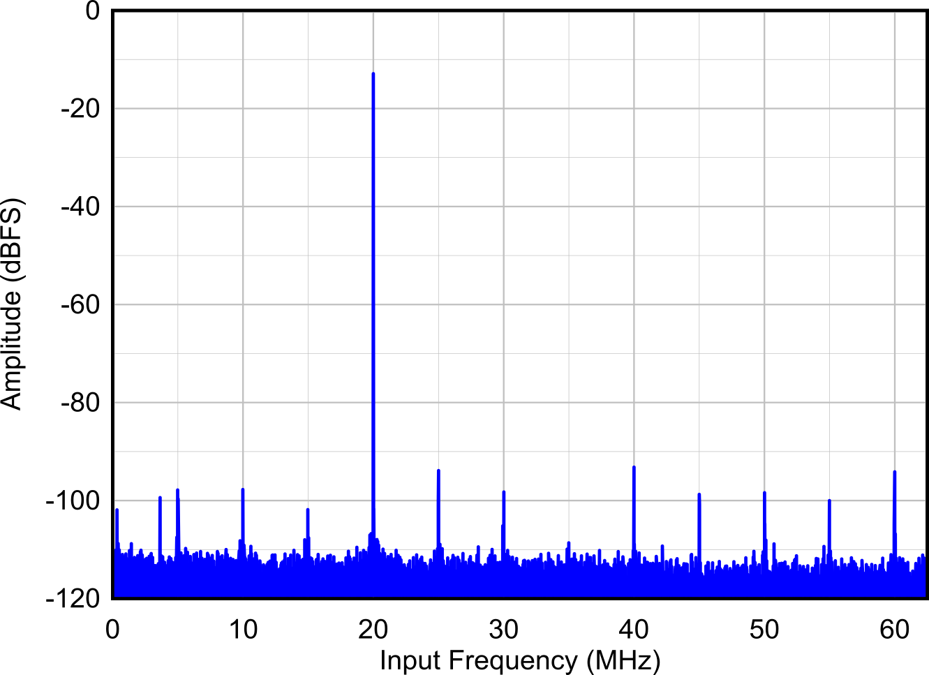
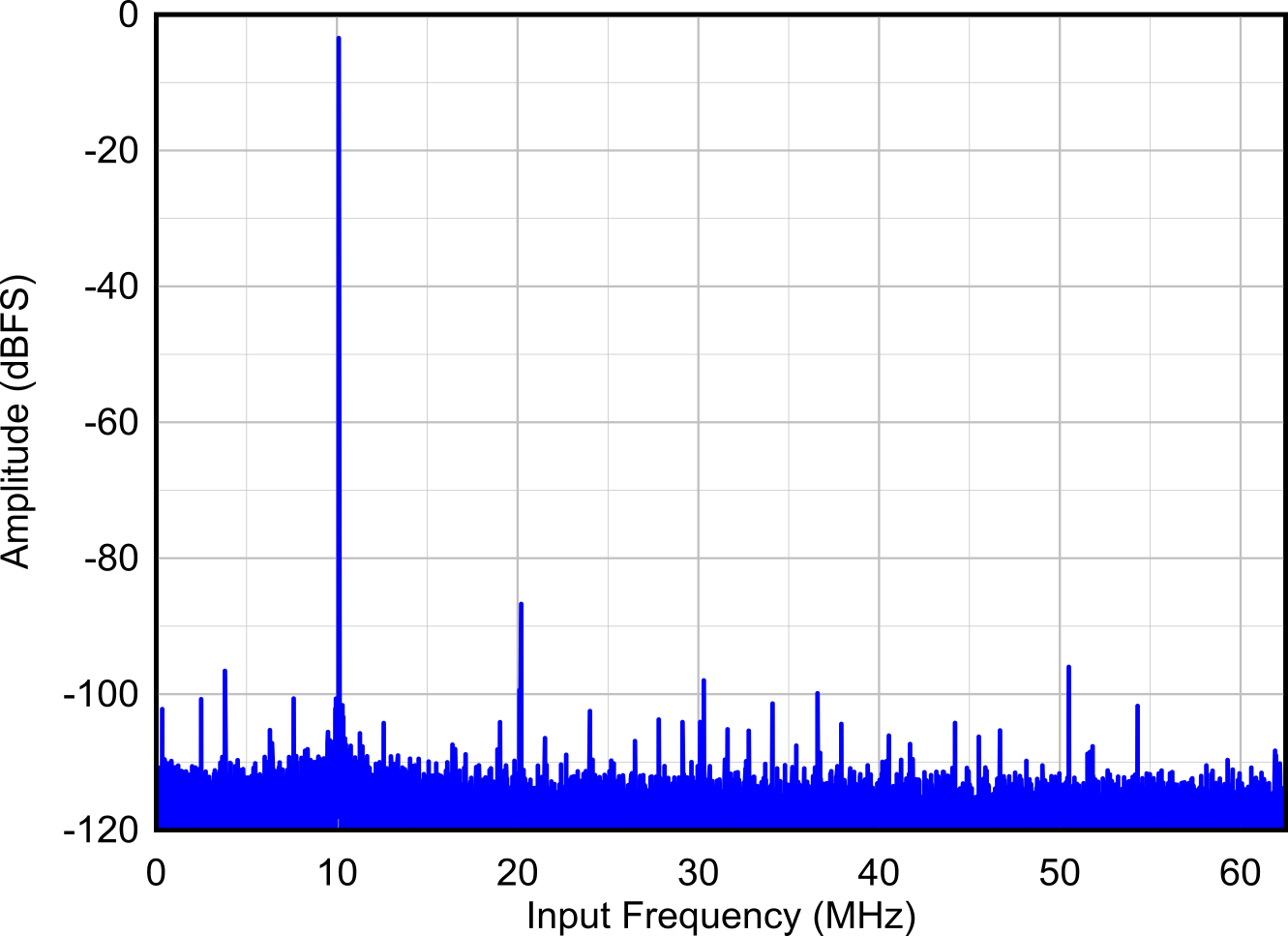
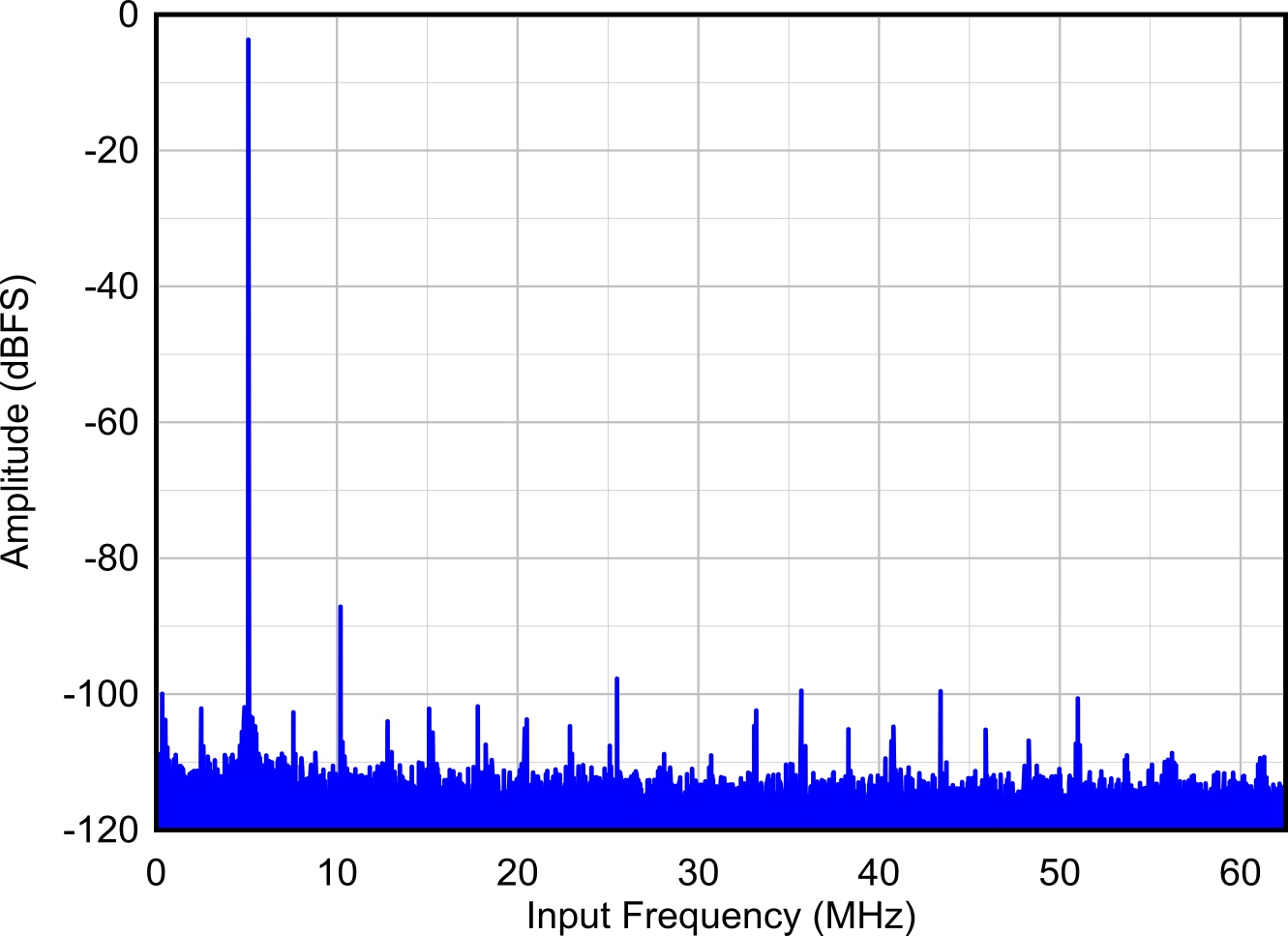
The following FFT plots show the performance of THS4541 driving the ADC3644 operated at 125 MSPS with a full-scale input at -1 dBFS. The FFT spectrum also shows the response of the low pass filter located between the THS4541 and the glitch filter with a 30 MHz corner frequency.
GUID-20211208-SS0I-P0SW-SQN9-HZB8TFH9RWSC-low.png
AIN = - 1 dBFS, SNR = 73.2 dBFS, SFDR = 84 dBFS
Figure 9-2 5 MHz FFT (THS4541 FDA)
GUID-20211208-SS0I-HCQV-SBFR-JB4RTKZ2D1VV-low.png
AIN = - 10 dBFS, SNR = 73.5 dBFS, SFDR = 90 dBFS
Figure 9-4 20 MHz FFT (THS4541 FDA)
GUID-20211208-SS0I-RPJQ-V5XJ-WQXNRNLF6JJG-low.png
AIN = - 1 dBFS, SNR = 73 dBFS, SFDR = 84 dBFS
Figure 9-3 10.1 MHz FFT (THS4541 FDA)