ZHCSNC3B February   2021  – October 2022 ADC3561 , ADC3562 , ADC3563

PRODUCTION DATA  

  1. 特性
  2. 应用
  3. 说明
  4. Revision History
  5. Pin Configuration and Functions
  6. Specifications
    1. 6.1  绝对最大额定值
    2. 6.2  ESD 等级
    3. 6.3  建议运行条件
    4. 6.4  热性能信息
    5. 6.5  电气特性 - 功耗
    6. 6.6  电气特征 - 直流规格
    7. 6.7  电气特征 - 交流规格
    8. 6.8  时序要求
    9. 6.9  Typical Characteristics - ADC3561
    10. 6.10 Typical Characteristics - ADC3562
    11. 6.11 Typical Characteristics - ADC3563
  7. Parameter Measurement Information
  8. Detailed Description
    1. 8.1 Overview
    2. 8.2 Functional Block Diagram
    3. 8.3 Feature Description
      1. 8.3.1 Analog Input
        1. 8.3.1.1 Analog Input Bandwidth
        2. 8.3.1.2 Analog Front End Design
          1. 8.3.1.2.1 Sampling Glitch Filter Design
          2. 8.3.1.2.2 Analog Input Termination and DC Bias
            1. 8.3.1.2.2.1 AC-Coupling
            2. 8.3.1.2.2.2 DC-Coupling
        3. 8.3.1.3 Auto-Zero Feature
      2. 8.3.2 Clock Input
        1. 8.3.2.1 Single Ended vs Differential Clock Input
        2. 8.3.2.2 Signal Acquisition Time Adjust
      3. 8.3.3 Voltage Reference
        1. 8.3.3.1 Internal voltage reference
        2. 8.3.3.2 External voltage reference (VREF)
        3. 8.3.3.3 External voltage reference with internal buffer (REFBUF)
      4. 8.3.4 Digital Down Converter
        1. 8.3.4.1 DDC MUX for Dual Band Decimation
        2. 8.3.4.2 Digital Filter Operation
        3. 8.3.4.3 FS/4 Mixing with Real Output
        4. 8.3.4.4 Numerically Controlled Oscillator (NCO) and Digital Mixer
        5. 8.3.4.5 Decimation Filter
        6. 8.3.4.6 SYNC
        7. 8.3.4.7 Output Formatting with Decimation
      5. 8.3.5 Digital Interface
        1. 8.3.5.1 Output Formatter
        2. 8.3.5.2 Output Bit Mapper
        3. 8.3.5.3 Output Scrambler
        4. 8.3.5.4 Output Interface/Mode Configuration
          1. 8.3.5.4.1 Configuration Example
        5. 8.3.5.5 Output Data Format
      6. 8.3.6 Test Pattern
    4. 8.4 Device Functional Modes
      1. 8.4.1 Normal operation
      2. 8.4.2 Power Down Options
    5. 8.5 Programming
      1. 8.5.1 Configuration using PINs only
      2. 8.5.2 Configuration using the SPI interface
        1. 8.5.2.1 Register Write
        2. 8.5.2.2 Register Read
    6. 8.6 Register Maps
      1. 8.6.1 Detailed Register Description
  9. Application Information Disclaimer
    1. 9.1 Typical Application
      1. 9.1.1 Design Requirements
      2. 9.1.2 Detailed Design Procedure
        1. 9.1.2.1 Input Signal Path
        2. 9.1.2.2 Sampling Clock
        3. 9.1.2.3 Voltage Reference
      3. 9.1.3 Application Curves
    2. 9.2 Initialization Set Up
      1. 9.2.1 Register Initialization During Operation
    3. 9.3 Power Supply Recommendations
    4. 9.4 Layout
      1. 9.4.1 Layout Guidelines
      2. 9.4.2 Layout Example
  10. 10Device and Documentation Support
    1. 10.1 Device Support
    2. 10.2 Documentation Support
    3. 10.3 接收文档更新通知
    4. 10.4 支持资源
    5. 10.5 Trademarks
    6. 10.6 Electrostatic Discharge Caution
    7. 10.7 术语表
  11. 11Mechanical, Packaging, and Orderable Information

封装选项

机械数据 (封装 | 引脚)
散热焊盘机械数据 (封装 | 引脚)
订购信息

Output Formatting with Decimation

When using decimation, the output data is formatted as shown in Figure 8-39 (complex decimation) and Figure 8-40 (real decimation).
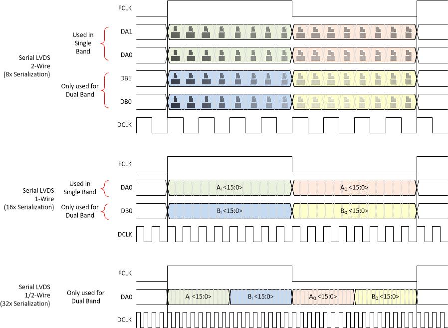
GUID-4926EBA4-1761-4795-BFD4-A22DEC061C1A-low.gifFigure 8-39 Output Data Format in Complex Decimation

Table 8-4 illustrates the output interface data rate along with the corresponding DCLK/DCLKIN and FCLK frequencies based on output resolution (R), number of SLVDS lanes (L) and complex decimation setting (N).

Furthermore the table shows an actual lane rate example for the 2-, 1- and 1/2-wire interface, 16-bit output resolution and complex decimation by 4.

Table 8-4 Serial LVDS Lane Rate Examples with Complex Decimation and 16-bit Output Resolution
DECIMATION SETTINGADC SAMPLING RATEOUTPUT RESOLUTION# of WIRESFCLKDCLKIN, DCLKDA/B0,1
NFSRLFS / N[DA/B0,1] / 2FS x 2 x R / L / N
465 MSPS16216.25 MHz130 MHz260 MHz
1260 MHz520 MHz
62.5 MSPS1/215.625 MHz500 MHz1000 MHz
GUID-E641007F-2044-47BD-B762-7089CD28040E-low.gif Figure 8-40 Output Data Format in Real Decimation

Table 8-5 illustrates the output interface data rate along with the corresponding DCLK/DCLKIN and FCLK frequencies based on output resolution (R), number of SLVDS lanes (L) and real decimation setting (M).

Furthermore the table shows an actual lane rate example for the 2-, 1- and 1/2-wire interface, 16-bit output resolution and real decimation by 4.

Table 8-5 Serial LVDS Lane Rate Examples with Real Decimation and 16-bit Output Resolution
DECIMATION SETTINGADC SAMPLING RATEOUTPUT RESOLUTION# of WIRESFCLKDCLKIN, DCLKDA/B0,1
MFSRLFS / M / 2 (L = 2)
FS / M (L = 1, 1/2)
[DA/B0,1] / 2FS x R / L / M
465 MSPS1628.125 MHz65 MHz130 MHz
116.25 MHz130 MHz260 MHz