SLUSBL4C August 2013 – October 2015 UCC27211A
PRODUCTION DATA.
- 1 Features
- 2 Applications
- 3 Description
- 4 Revision History
- 5 Description (continued)
- 6 Pin Configuration and Functions
-
7 Specifications
- 7.1 Absolute Maximum Ratings
- 7.2 ESD Ratings
- 7.3 Recommended Operating Conditions
- 7.4 Thermal Information
- 7.5 Electrical Characteristics
- 7.6 Switching Characteristics: Propagation Delays
- 7.7 Switching Characteristics: Delay Matching
- 7.8 Switching Characteristics: Output Rise and Fall Time
- 7.9 Switching Characteristics: Miscellaneous
- 7.10 Typical Characteristics
- 8 Detailed Description
- 9 Application and Implementation
- 10Power Supply Recommendations
- 11Layout
- 12Device and Documentation Support
- 13Mechanical, Packaging, and Orderable Information
Package Options
Mechanical Data (Package|Pins)
- DRM|8
Thermal pad, mechanical data (Package|Pins)
- DRM|8
Orderable Information
1 Features
- Drives Two N-Channel MOSFETs in High-Side and Low-Side Configuration With Independent Inputs
- Maximum Boot Voltage 120-V DC
- 4-A Sink, 4-A Source Output Currents
- 0.9-Ω Pullup and Pulldown Resistance
- Input Pins Can Tolerate –10 V to +20 V and are Independent of Supply Voltage Range
- TTL or Pseudo-CMOS Compatible Input Versions
- 8-V to 17-V VDD Operating Range, (20-V ABS MAX)
- 7.2-ns Rise and 5.5-ns Fall Time With 1000-pF Load
- Fast Propagation Delay Times (20-ns typical)
- 4-ns Delay Matching
- Symmetrical Undervoltage Lockout for High-Side and Low-Side Driver
- All Industry Standard Packages Available
- SOIC-8
- 4-mm × 4-mm SON-8
- 4-mm × 4-mm SON-10
- Specified from –40 to +140°C
2 Applications
- Power Supplies for Telecom, Datacom, and Merchant
- Half-Bridge and Full-Bridge Converters
- Push-Pull Converters
- High Voltage Synchronous-Buck Converters
- Two-Switch Forward Converters
- Active-Clamp Forward Converters
- Class-D Audio Amplifiers
3 Description
The UCC27211A driver is based on the popular UCC27201 MOSFET drivers; but, this device offers several significant performance improvements. Peak output pullup and pulldown current has been increased to 4-A source and 4-A sink, and pullup and pulldown resistance have been reduced to 0.9 Ω, and thereby allows for driving large power MOSFETs with minimized switching losses during the transition through the Miller Plateau of the MOSFET. The input structure can directly handle –10 VDC, which increases robustness and also allows direct interface to gate-drive transformers without using rectification diodes. The inputs are also independent of supply voltage and have a 20-V maximum rating.
Device Information(1)
| PART NUMBER | PACKAGE | BODY SIZE (NOM) |
|---|---|---|
| UCC27211A | SOIC (8) | 4.90 mm × 3.91 mm |
| VSON (8) | 4.00 mm × 4.00 mm |
- For all available packages, see the orderable addendum at the end of the data sheet.
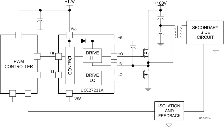
Typical Application Diagram

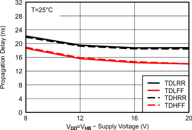
Propagation Delays vs Supply Voltage
