SCDS339B January 2013 – April 2017 TS3A5223
PRODUCTION DATA.
- 1 Features
- 2 Applications
- 3 Description
- 4 Revision History
- 5 Pin Configuration and Functions
- 6 Specifications
- 7 Parameter Measurement Information
- 8 Detailed Description
- 9 Application and Implementation
- 10Power Supply Recommendations
- 11Layout
- 12Device and Documentation Support
- 13Mechanical, Packaging, and Orderable Information
Package Options
Mechanical Data (Package|Pins)
- RSW|10
Thermal pad, mechanical data (Package|Pins)
Orderable Information
1 Features
- Low ON Resistance Switches
- 0.45 Ω (Typical) at 3.6 V
- 0.85 Ω (Typical) at 1.8 V
- Wide Supply Range: 1.65 V to 3.6 V
- 1.0 V Compatible Logic Interface
- High Switch Bandwidth 80 MHz
- 0.01% THD Across Entire Band
- Specified min Break-before-make
- Bi-directional Switching
- –75 dB Channel-to-Channel Crosstalk
- –70 dB Channel-to-Channel OFF Isolation of Very Low Power Dissipation and Leakage Currents
- Very Small QFN-10 Package: 1.8 mm × 1.4 mm
- ESD Protection on all Pins
- 2 kV HBM, 500 V CDM
2 Applications
- Portable Electronics
- Smartphones, Tablets
- Home Electronics
- Wireline Communication
3 Description
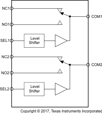
The TS3A5223 is a high-speed 2-channel analog switch with break-before-make and bi-directional signal switching capability. The TS3A5223 can be used as a dual 2:1 multiplexer or a 1:2 dual de-multiplexer.
The TS3A5223 offers very low ON resistance, very low THD, channel-to-channel crosstalk and very high OFF isolation. These features make TS3A5223 suitable for application in Audio signal routing and switching applications.
The TS3A5223 control logic supports 1 V – 3.6 V CMOS logic levels. The logic interface allows direct interface with a wide range of CPUs and microcontrollers without increasing the current drawn from supply (ICC) and thus lowering power consumption.
Device Information(1)
| PART NUMBER | PACKAGE | BODY SIZE (NOM) |
|---|---|---|
| TS3A5223 | µQFN (10) | 1.80 mm x 1.40 mm |
- For all available packages, see the orderable addendum at the end of the data sheet.
Functional Diagram
