SCDS358B November 2014 – February 2015 TS3A227E
PRODUCTION DATA.
- 1 Features
- 2 Applications
- 3 Description
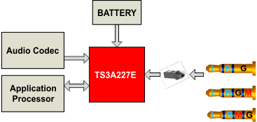
- 4 Simplified Schematic
- 5 Revision History
- 6 Pin Configuration and Functions
- 7 Specifications
- 8 Parameter Measurement Information
-
9 Detailed Description
- 9.1 Overview
- 9.2 Functional Block Diagram
- 9.3 Feature Description
- 9.4 Device Functional Modes
- 9.5 Register Maps
- 9.6
Register Field Descriptions
- 9.6.1 Device ID Register Field Descriptions (Address 00h)
- 9.6.2 Interrupt Register Field Descriptions (Address 01h)
- 9.6.3 Key Press Interrupt Register Field Descriptions (Address 02h)
- 9.6.4 Interrupt Disable Register Field Descriptions (Address 03h)
- 9.6.5 Device Settings Field Descriptions (Address 04h)
- 9.6.6 Key Press Settings 1 Field Descriptions (Address 05h)
- 9.6.7 Key Press Settings 2 Field Descriptions (Address 06h)
- 9.6.8 Switch Control 1 Field Descriptions (Address 07h)
- 9.6.9 Switch Control 2 Field Descriptions (Address 08h)
- 9.6.10 Switch Status 1 Field Descriptions (Address 09h)
- 9.6.11 Switch Status 2 Field Descriptions (Address 0Ah)
- 9.6.12 Detection Results Field Descriptions (Address 0Bh)
- 9.6.13 ADC Output Field Descriptions (Address 0Ch)
- 9.6.14 Threshold 1 Field Descriptions (Address 0Dh)
- 9.6.15 Threshold 2 Field Descriptions (Address 0Eh)
- 9.6.16 Threshold 3 Field Descriptions (Address 0Fh)
- 10Application and Implementation
- 11Power Supply Recommendations
- 12Layout
- 13Device and Documentation Support
- 14Mechanical, Packaging, and Orderable Information
Package Options
Mechanical Data (Package|Pins)
Thermal pad, mechanical data (Package|Pins)
- RVA|16
Orderable Information
1 Features
- Supple Range of 2.5 V to 4.5 V
- Accessory Insertion/Removal Detection with Adjustable De-bounce Timings
- Accessory Configuration Detection:
- Stereo 3-pole Headphone
- 4-pole Standard Headset with MIC on Sleeve
- 4-pole OMTP Headset with MIC on Ring2
- Key Press Detection for Up to 4 Keys
- Ultra Low Ground FET RON of 60 mΩ
- Power Off Noise Removal
- Isolation of MICBIAS From Audio Jack to Remove Click/Pop Noise
- Integrated Codec Sense Line
- Manual I2C Control
- FM Transmission Capability
- Dual Small Package Options
- 16 Pin DSBGA
- 16 Pin QFN
2 Applications
- Mobile Phones
- Tablets
- Notebooks and Ultrabooks
- Anywhere a 3.5 mm Audio Jack is Used
3 Description
The TS3A227E is an autonomous audio accessory detection and configuration switch that detects 3-pole or 4-pole audio accessories and configures internal switches to route the signals accordingly.
The internal ground FETS of the TS3A227E have an ultra-low RON of 60 mΩ to minimize crosstalk impact. The ground FETs are also designed to pass FM signals, making it possible to use the ground line of the accessory as an FM antenna in mobile audio applications.
Internal isolation switches allow the TS3A227E to remove the click/pop noise that can be generated during and insertion or removal of an audio accessory. In addition depletion FETs prevent a floating ground while the device is unpowered, removing the humming noise present when leaving accessories plugged into an unpowered system.
A low-power sleep mode is provided which shuts down internal circuitry to achieve very low quiescent current draw when no headset is inserted.
The TS3A227E features integrated key press detection for detecting up to 4 keys with press and release support.
Manual I2C control allows the TS3A227E to adapt to application needs by providing control over de-bounce settings and switch states.
Device Information(1)
| PART NUMBER | PACKAGE | BODY SIZE (NOM) |
|---|---|---|
| TS3A227E | QFN (16) | 3.50 mm × 3.50 mm |
| DSBGA (16) | 1.79 mm × 1.79 mm |
- For all available packages, see the orderable addendum at the end of the datasheet.
4 Simplified Schematic