SLVSAN6B February 2011 – September 2016 TPS61181A
PRODUCTION DATA.
- 1 Features
- 2 Applications
- 3 Description
- 4 Revision History
- 5 Device Comparison Table
- 6 Pin Configuration and Functions
- 7 Specifications
- 8 Detailed Description
- 9 Application and Implementation
- 10Power Supply Recommendations
- 11Layout
- 12Device And Documentation Support
- 13Mechanical, Packaging, and Orderable Information
Package Options
Mechanical Data (Package|Pins)
- RTE|16
Thermal pad, mechanical data (Package|Pins)
- RTE|16
Orderable Information
1 Features
- 4.5-V to 24-V Input Voltage
- 38-V Maximum Output Voltage
- Integrated 1.5-A/40-V MOSFET
- 1-MHz Switching Frequency
- Adaptive Boost Output to WLED Voltages
- Small External Components
- Integrated Loop Compensation
- Six Current Sinks of 30 mA
- Up to 10 WLED in Series
- 1% Typical Current Matching and Accuracy
- Up to 1000:1 PWM Brightness Dimming
- Minimized Output Ripple Under PWM Dimming
- Driver for Input/Output Isolation PFET
- True Shutdown
- Overvoltage Protection
- WLED Open and Short Protection
- Built-in Soft Start
2 Applications
- Notebook LCD Display Backlight
- UMPC LCD Display Backlight
- Backlight for Media Form Factor LCD Display
3 Description
The TPS61181A device provides highly integrated solutions for media-size LCD backlighting. The six current sink regulators provide high-precision current regulation and matching. In total, the device can support up to 60 WLEDs.
The devices support pulse width modulation (PWM) brightness dimming. During dimming, the WLED current is turned on/off at the duty cycle and frequency, determined by the PWM signal input to the DCRTL pin. The TPS61181A device is designed to minimize the output AC ripple across a wide dimming duty cycle and frequency range and also reduces the audible noise from the output ceramic capacitors.
The TPS61181A device provides a driver output for an external PFET connected between the input and inductor. During short circuit or overcurrent conditions, the device turns off the external PFET and disconnects the battery from the WLEDs. The PFET is also turned off during device shutdown (thereby giving true shutdown) to prevent any leakage current from the battery. The device integrates overvoltage protection, soft-start and thermal shutdown and has a built-in linear regulator for the device supply.
Device Information(1)
| PART NUMBER | PACKAGE | BODY SIZE (NOM) |
|---|---|---|
| TPS61181A | WQFN (16) | 3.00 mm × 3.00 mm |
space
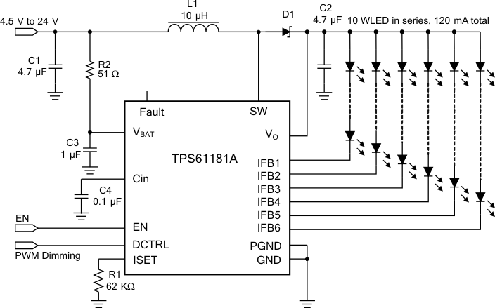
TPS61181A Typical Application
