SLVSE71 September 2017 TPS565201
PRODUCTION DATA.
- 1 Features
- 2 Applications
- 3 Description
- 4 Revision History
- 5 Pin Configuration and Functions
- 6 Specifications
- 7 Detailed Description
- 8 Application and Implementation
- 9 Power Supply Recommendations
- 10Layout
- 11Device and Documentation Support
- 12Mechanical, Packaging, and Orderable Information
Package Options
Mechanical Data (Package|Pins)
- DDC|6
Thermal pad, mechanical data (Package|Pins)
Orderable Information
1 Features
- 5-A Maximum Output Current
- Integrated 31-mΩ and 16-mΩ FETs
- D-CAP2™ Mode Control with Fast Transient Response
- Input Voltage Range: 4.5 V to 17 V
- Output Voltage Range: 0.76 V to 7 V
- High Efficiency at Light Loads with Pulse-skipping Eco-mode™
- 500-kHz Switching Frequency
- ≤1 µA Shutdown Current
- 1% Feedback Voltage Accuracy
- Startup from Pre-Biased Output Voltage
- Cycle-by-Cycle Current Limit
- Hiccup-mode Overcurrent Protection
- Non-Latch UVP, UVLO and TSD Protections
2 Applications
- Digital TV Power Supply
- High Definition Blu-ray™ Disc Players
- Networking Home Terminal
- Digital Set Top Box (STB)
- Surveillance
3 Description
The TPS565201 is a simple, easy-to-use, 5-A synchronous step-down converter.
The device is optimized to operate with minimum external component counts and also optimized to achieve low standby current.
This switch mode power supply (SMPS) device employs D-CAP2™ control, which provides fast transient response and requires no external compensation components. D-CAP2 also allows the use of low-equivalent series resistance (ESR) specialty polymer capacitors and ceramic output capacitors.
The TPS565201 operates in pulse skip mode, maintaining high efficiency during light load operation.
The TPS565201 device is available in a 6-pin 1.6-mm × 2.9-mm SOT (DDC) package, and operates over a –40°C to 125°C junction temperature range.
Device Information(1)
| PART NUMBER | PACKAGE | BODY SIZE (NOM) |
|---|---|---|
| TPS565201 | DDC (6) | 1.60 mm × 2.90 mm |
- For all available packages, see the orderable addendum at the end of the data sheet.
spacer
spacer
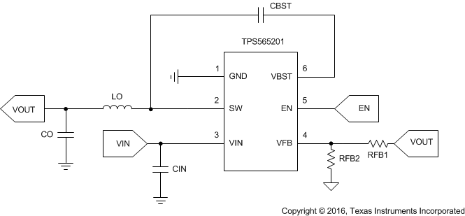
Simplified Schematic

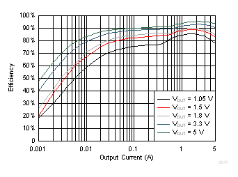
TPS565201 Efficiency
