SBVS323 September 2017 TLV742P
PRODUCTION DATA.
- 1 Features
- 2 Applications
- 3 Description
- 4 Revision History
- 5 Pin Configuration and Functions
- 6 Specifications
- 7 Detailed Description
- 8 Application and Implementation
- 9 Power Supply Recommendations
- 10Layout
- 11Device and Documentation Support
- 12Mechanical, Packaging, and Orderable Information
Package Options
Refer to the PDF data sheet for device specific package drawings
Mechanical Data (Package|Pins)
- DQN|4
Thermal pad, mechanical data (Package|Pins)
- DQN|4
Orderable Information
1 Features
- Input Voltage Range From 2 V to 5.5 V
- Fixed-Output Voltage Combinations Possible From 0.85 V to 5 V in 50-mV Steps(1)
- 0.5% Typical Accuracy
- High PSRR:
- 55 dB at 1 MHz
- IQ When Enabled: 25 µA
- IQ When Disabled: 1 µA
- Active Output Discharge
- Thermal Shutdown and Overcurrent Protection
- Package:
- 1-mm × 1-mm DQN (X2SON)
2 Applications
- Point of Sale
- Camera and Machine Vision Modules
- Gaming and Toys
- Building Automation and Video Surveillance
- TVs and Set-Top Boxes
3 Description
The TLV742P series of low-dropout linear voltage regulators (LDOs) are optimized to providing excellent performance by supporting a wide output voltage range. The LDOs can directly regulate a single cell Li-ion battery input-to-output voltage as low as 0.85 V. If used to post-regulate a DC-DC converter output, the high PSRR of 55 dB at 1 MHz suppresses ripple to provide a stable low-noise, well-regulated VOUT.
The TLV742P has an active output discharge feature that helps ensure the output is kept low while the system is disabled, in standby mode, or in sleep mode. Additionally, overcurrent protection is present to protect the device in the event of an output short along with thermal shutdown to prevent overheating.
The TLV742P series of voltage regulators are available in a 1 mm × 1 mm X2SON package to minimize PCB area.
Device Information(1)
| PART NUMBER | PACKAGE | BODY SIZE (NOM) |
|---|---|---|
| TLV742P | X2SON (4) | 1.00 mm × 1.00 mm |
- For all available packages, see the orderable addendum at the end of the data sheet.
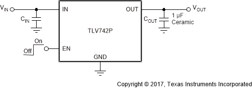
Typical Application Circuit
