SLLSEN8C September 2015 – June 2017 TL16C752D
PRODUCTION DATA.
- 1 Features
- 2 Applications
- 3 Description
- 4 Revision History
- 5 Description (continued)
- 6 Pin Configurations and Function
- 7 Specifications
-
8 Detailed Description
- 8.1 Overview
- 8.2 Functional Block Diagrams
- 8.3
Feature Description
- 8.3.1
Functional Description
- 8.3.1.1 Trigger Levels
- 8.3.1.2 Hardware Flow Control
- 8.3.1.3 Auto-RTS
- 8.3.1.4 Auto-CTS
- 8.3.1.5 Software Flow Control
- 8.3.1.6 Software Flow Control Example
- 8.3.1.7 Reset
- 8.3.1.8 Interrupts
- 8.3.1.9 Interrupt Mode Operation
- 8.3.1.10 Polled Mode Operation
- 8.3.1.11 Break and Timeout Conditions
- 8.3.1.12 Programmable Baud Rate Generator
- 8.3.1
Functional Description
- 8.4 Device Functional Modes
- 8.5
Register Maps
- 8.5.1 Principals of Operation
- 8.5.2 Receiver Holding Register (RHR)
- 8.5.3 Transmit Holding Register (THR)
- 8.5.4 FIFO Control Register (FCR)
- 8.5.5 Line Control Register (LCR)
- 8.5.6 Line Status Register (LSR)
- 8.5.7 Modem Control Register (MCR)
- 8.5.8 Modem Status Register (MSR)
- 8.5.9 Interrupt Enable Register (IER)
- 8.5.10 Interrupt Identification Register (IIR)
- 8.5.11 Enhanced Feature Register (EFR)
- 8.5.12 Divisor Latches (DLL, DLH)
- 8.5.13 Transmission Control Register (TCR)
- 8.5.14 Trigger Level Register (TLR)
- 8.5.15 FIFO Ready Register
- 8.5.16 Alternate Function Register (AFR)
- 8.5.17 RS-485 Mode
- 8.5.18 IrDA Overview
- 8.5.19 IrDA Encoder Function
- 9 Application and Implementation
- 10Power Supply Recommendations
- 11Layout
- 12Device and Documentation Support
- 13Mechanical, Packaging, and Orderable Information
Package Options
Mechanical Data (Package|Pins)
- PFB|48
Thermal pad, mechanical data (Package|Pins)
- PFB|48
Orderable Information
1 Features
- Pin Compatible With TL16C2550 With Enhanced Features Provided Through an Improved FIFO Register
- Supports Wide Supply Voltage Range of 1.62 V to 5.5 V
- Characterized for Operation from –40°C to 85°C
- 64-Byte Transmit/Receive FIFO
- Software-Selectable Baud-Rate Generator
- Programmable and Selectable Transmit and Receive FIFO Trigger Levels for DMA, Interrupt Generation, and Software or Hardware Flow Control
- Software/Hardware Flow Control
- Programmable Xon and Xoff Characters With Optional Xon Any Character
- Programmable Auto-RTS and Auto-CTS-Modem Control Functions (CTS, RTS, DSR, DTR, RI, and CD)
- DMA Signaling Capability for Both Received and Transmitted Data on PN Package
- RS-485 Mode Support
- Infrared Data Association (IrDA) Capability
- Programmable Sleep Mode
- Programmable Serial Interface Characteristics
- 5, 6, 7, or 8-Bit Characters With 1, 1.5, or 2 Stop Bit Generation
- Even, Odd, or No Parity Bit Generation and Detection
- False Start Bit and Line Break Detection
- Internal Test and Loopback Capabilities
- SC16C752B and XR16M752 Pin Compatible With Additional Enhancements
2 Applications
- Automotive Infotainment
- Mobile Devices
- Communications Equipment
- White Goods
- Industrial Computing
3 Description
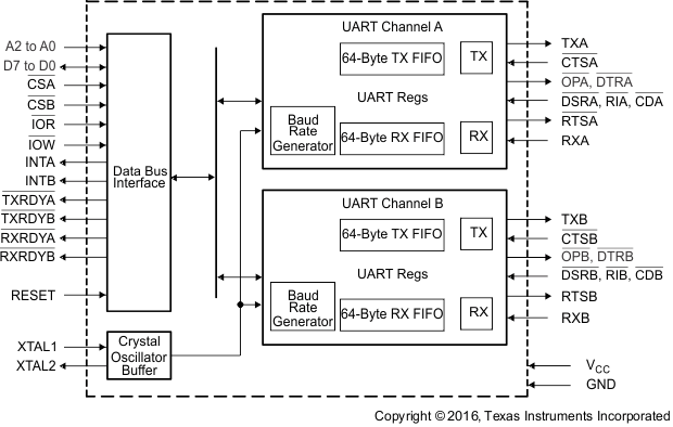
The TL16C752D is a dual universal asynchronous receiver transmitter (UART) with 64-byte FIFOs, automatic hardware and software flow control, and data rates up to 3 Mbps. The device offers enhanced features. It has a transmission character control register (TCR) that stores received FIFO threshold level to start or stop transmission during hardware and software flow control.
With the FIFO RDY register, the software gets the status of TXRDY or RXRDY for all two ports in one access. On-chip status registers provide the user with error indications, operational status, and modem interface control. System interrupts may be tailored to meet user requirements. An internal loop-back capability allows onboard diagnostics. The TL16C752D incorporates the functionality of two UARTs, each UART having its own register set and FIFOs.
Device Information(1)
| PART NUMBER | PACKAGE | BODY SIZE (NOM) |
|---|---|---|
| TL16C752D | TQFP (48) | 7.00 mm × 7.00 mm |
- For all available packages, see the orderable addendum at the end of the data sheet.
Block Diagram
