SLASEG7 December 2016 TAS5780M
PRODUCTION DATA.
- 1 Features
- 2 Applications
- 3 Description
- 4 Revision History
- 5 Device Comparison Table
- 6 Pin Configuration and Functions
-
7 Specifications
- 7.1 Absolute Maximum Ratings
- 7.2 ESD Ratings
- 7.3 Recommended Operating Conditions
- 7.4 Thermal Information
- 7.5 Electrical Characteristics
- 7.6 Power Dissipation Characteristics
- 7.7 MCLK Timing
- 7.8 Serial Audio Port Timing - Slave Mode
- 7.9 Serial Audio Port Timing - Master Mode
- 7.10 I2C Bus Timing - Standard
- 7.11 I2C Bus Timing - Fast
- 7.12 SPK_MUTE Timing
- 7.13 Typical Characteristics
- 8 Parametric Measurement Information
-
9 Detailed Description
- 9.1 Overview
- 9.2 Functional Block Diagram
- 9.3
Feature Description
- 9.3.1 Power-on-Reset (POR) Function
- 9.3.2 Device Clocking
- 9.3.3
Serial Audio Port
- 9.3.3.1 Clock Master Mode from Audio Rate Master Clock
- 9.3.3.2 Clock Master from a Non-Audio Rate Master Clock
- 9.3.3.3 Clock Slave Mode with 4-Wire Operation (SCLK, MCLK, LRCK/FS, SDIN)
- 9.3.3.4 Clock Slave Mode with SCLK PLL to Generate Internal Clocks (3-Wire PCM)
- 9.3.3.5 Serial Audio Port - Data Formats and Bit Depths
- 9.3.3.6 Input Signal Sensing (Power-Save Mode)
- 9.3.4 Enable Device
- 9.3.5 Volume Control
- 9.3.6 Adjustable Amplifier Gain and Switching Frequency Selection
- 9.3.7
Error Handling and Protection Suite
- 9.3.7.1 Device Overtemperature Protection
- 9.3.7.2 SPK_OUTxx Overcurrent Protection
- 9.3.7.3 Internal VAVDD Undervoltage-Error Protection
- 9.3.7.4 Internal VPVDD Undervoltage-Error Protection
- 9.3.7.5 Internal VPVDD Overvoltage-Error Protection
- 9.3.7.6 External Undervoltage-Error Protection
- 9.3.7.7 Internal Clock Error Notification (CLKE)
- 9.3.8 GPIO Port and Hardware Control Pins
- 9.3.9 I2C Communication Port
- 9.4 Device Functional Modes
- 9.5
Programming
- 9.5.1 Audio Processing Features
- 9.5.2 Processing Block Description
- 9.5.3 Other Processing Block Features
- 9.5.4 Checksum
- 10Application and Implementation
- 11Power Supply Recommendations
- 12Layout
-
13Register Maps
- 13.1
Registers - Page 0
- 13.1.1 Register 1 (0x01)
- 13.1.2 Register 2 (0x02)
- 13.1.3 Register 3 (0x03)
- 13.1.4 Register 4 (0x04)
- 13.1.5 Register 5 (0x05)
- 13.1.6 Register 6 (0x06)
- 13.1.7 Register 7 (0x07)
- 13.1.8 Register 8 (0x08)
- 13.1.9 Register 9 (0x09)
- 13.1.10 Register 10 (0x0A)
- 13.1.11 Register 12 (0x0C)
- 13.1.12 Register 13 (0x0D)
- 13.1.13 Register 14 (0x0E)
- 13.1.14 Register 15 (0x0F)
- 13.1.15 Register 16 (0x10)
- 13.1.16 Register 17 (0x11)
- 13.1.17 Register 18 (0x12)
- 13.1.18 Register 19 (0x13)
- 13.1.19 Register 20 (0x14)
- 13.1.20 Register 21 (0x15)
- 13.1.21 Register 22 (0x16)
- 13.1.22 Register 23 (0x17)
- 13.1.23 Register 24 (0x18)
- 13.1.24 Register 25 (0x19)
- 13.1.25 Register 26 (0x1A)
- 13.1.26 Register 27 (0x1B)
- 13.1.27 Register 28 (0x1C)
- 13.1.28 Register 29 (0x1D)
- 13.1.29 Register 30 (0x1E)
- 13.1.30 Register 31 (0x1F)
- 13.1.31 Register 32 (0x20)
- 13.1.32 Register 33 (0x21)
- 13.1.33 Register 34 (0x22)
- 13.1.34 Register 35 (0x23)
- 13.1.35 Register 37 (0x25)
- 13.1.36 Register 38 (0x26)
- 13.1.37 Register 39 (0x27)
- 13.1.38 Register 40 (0x28)
- 13.1.39 Register 41 (0x29)
- 13.1.40 Register 42 (0x2A)
- 13.1.41 Register 43 (0x2B)
- 13.1.42 Register 44 (0x2C)
- 13.1.43 Register 45 (0x2D)
- 13.1.44 Register 46 (0x2E)
- 13.1.45 Register 47 (0x2F)
- 13.1.46 Register 48 (0x30)
- 13.1.47 Register 49 (0x31)
- 13.1.48 Register 50 (0x32)
- 13.1.49 Register 51 (0x33)
- 13.1.50 Register 52 (0x34)
- 13.1.51 Register 53 (0x35)
- 13.1.52 Register 59 (0x3B)
- 13.1.53 Register 60 (0x3C)
- 13.1.54 Register 61 (0x3D)
- 13.1.55 Register 62 (0x3E)
- 13.1.56 Register 63 (0x3F)
- 13.1.57 Register 64 (0x40)
- 13.1.58 Register 65 (0x41)
- 13.1.59 Register 66 (0x42)
- 13.1.60 Register 67 (0x43)
- 13.1.61 Register 68 (0x44)
- 13.1.62 Register 69 (0x45)
- 13.1.63 Register 70 (0x46)
- 13.1.64 Register 71 (0x47)
- 13.1.65 Register 72 (0x48)
- 13.1.66 Register 73 (0x49)
- 13.1.67 Register 74 (0x4A)
- 13.1.68 Register 75 (0x4B)
- 13.1.69 Register 76 (0x4C)
- 13.1.70 Register 78 (0x4E)
- 13.1.71 Register 79 (0x4F)
- 13.1.72 Register 80 (0x50)
- 13.1.73 Register 81 (0x51)
- 13.1.74 Register 82 (0x52)
- 13.1.75 Register 83 (0x53)
- 13.1.76 Register 84 (0x54)
- 13.1.77 Register 85 (0x55)
- 13.1.78 Register 86 (0x56)
- 13.1.79 Register 87 (0x57)
- 13.1.80 Register 88 (0x58)
- 13.1.81 Register 89 (0x59)
- 13.1.82 Register 91 (0x5B)
- 13.1.83 Register 92 (0x5C)
- 13.1.84 Register 93 (0x5D)
- 13.1.85 Register 94 (0x5E)
- 13.1.86 Register 95 (0x5F)
- 13.1.87 Register 96 (0x60)
- 13.1.88 Register 97 (0x61)
- 13.1.89 Register 98 (0x62)
- 13.1.90 Register 99 (0x63)
- 13.1.91 Register 100 (0x64)
- 13.1.92 Register 101 (0x65)
- 13.1.93 Register 102 (0x66)
- 13.1.94 Register 103 (0x67)
- 13.1.95 Register 104 (0x68)
- 13.1.96 Register 105 (0x69)
- 13.1.97 Register 106 (0x6A)
- 13.1.98 Register 107 (0x6B)
- 13.1.99 Register 108 (0x6C)
- 13.1.100 Register 109 (0x6D)
- 13.1.101 Register 110 (0x6E)
- 13.1.102 Register 111 (0x6F)
- 13.1.103 Register 112 (0x70)
- 13.1.104 Register 113 (0x71)
- 13.1.105 Register 114 (0x72)
- 13.1.106 Register 115 (0x73)
- 13.1.107 Register 118 (0x76)
- 13.1.108 Register 119 (0x77)
- 13.1.109 Register 120 (0x78)
- 13.1.110 Register 121 (0x79)
- 13.2
Registers - Page 1
- 13.2.1 Register 1 (0x01)
- 13.2.2 Register 2 (0x02)
- 13.2.3 Register 3 (0x03)
- 13.2.4 Register 4 (0x04)
- 13.2.5 Register 5 (0x05)
- 13.2.6 Register 6 (0x06)
- 13.2.7 Register 7 (0x07)
- 13.2.8 Register 8 (0x08)
- 13.2.9 Register 9 (0x09)
- 13.2.10 Register 10 (0x0A)
- 13.2.11 Register 11 (0x0B)
- 13.2.12 Register 12 (0x0C)
- 13.2.13 Register 13 (0x0D)
- 13.2.14 Register 14 (0x0E)
- 13.2.15 Register 15 (0x0F)
- 13.3
Registers - Page 253
- 13.3.1 Register 1 (0x01)
- 13.3.2 Register 2 (0x02)
- 13.3.3 Register 3 (0x03)
- 13.3.4 Register 4 (0x04)
- 13.3.5 Register 5 (0x05)
- 13.3.6 Register 6 (0x06)
- 13.3.7 Register 7 (0x07)
- 13.3.8 Register 8 (0x08)
- 13.3.9 Register 9 (0x09)
- 13.3.10 Register 10 (0x0A)
- 13.3.11 Register 11 (0x0B)
- 13.3.12 Register 12 (0x0C)
- 13.3.13 Register 13 (0x0D)
- 13.3.14 Register 14 (0x0E)
- 13.3.15 Register 15 (0x0F)
- 13.3.16 Register 16 (0x10)
- 13.3.17 Register 17 (0x11)
- 13.3.18 Register 18 (0x12)
- 13.3.19 Register 19 (0x13)
- 13.3.20 Register 20 (0x14)
- 13.3.21 Register 21 (0x15)
- 13.3.22 Register 2 (0x16)
- 13.3.23 Register 23 (0x17)
- 13.3.24 Register 24 (0x18)
- 13.3.25 Register 25 (0x19)
- 13.3.26 Register 26 (0x1A)
- 13.3.27 Register 27 (0x1B)
- 13.3.28 Register 28 (0x1C)
- 13.3.29 Register 29 (0x1D)
- 13.3.30 Register 30 (0x1E)
- 13.3.31 Register 31 (0x1F)
- 13.3.32 Register 32 (0x20)
- 13.3.33 Register 33 (0x21)
- 13.3.34 Register 34 (0x22)
- 13.3.35 Register 35 (0x23)
- 13.3.36 Register 36 (0x24)
- 13.3.37 Register 37 (0x25)
- 13.3.38 Register 38 (0x26)
- 13.3.39 Register 39 (0x27)
- 13.3.40 Register 40 (0x28)
- 13.3.41 Register 41 (0x29)
- 13.3.42 Register 42 (0x2A)
- 13.3.43 Register 43 (0x2B)
- 13.3.44 Register 44 (0x2C)
- 13.3.45 Register 63 (0x3F)
- 13.3.46 Register 64 (0x40)
- 13.3.47 Register 65 (0x41)
- 13.3.48 Register 70 (0x46)
- 13.3.49 Register 71 (0x47)
- 13.3.50 Register 72 (0x48)
- 13.3.51 Register 73 (0x49)
- 13.3.52 Register 74 (0x4A)
- 13.3.53 Register 75 (0x4B)
- 13.3.54 Register 76 (0x4C)
- 13.3.55 Register 77 (0x4D)
- 13.3.56 Register 78 (0x4E)
- 13.3.57 Register 79 (0x4F)
- 13.3.58 Register 80 (0x50)
- 13.3.59 Register 81 (0x51)
- 13.3.60 Register 82 (0x52)
- 13.3.61 Register 83 (0x53)
- 13.3.62 Register 84 (0x54)
- 13.3.63 Register 85 (0x55)
- 13.3.64 Register 86 (0x56)
- 13.3.65 Register 87 (0x57)
- 13.3.66 Register 88 (0x58)
- 13.3.67 Register 89 (0x59)
- 13.3.68 Register 90 (0x5A)
- 13.3.69 Register 91 (0x5B)
- 13.3.70 Register 92 (0x5C)
- 13.3.71 Register 93 (0x5D)
- 13.4 DSP Memory Map
- 13.1
Registers - Page 0
- 14Device and Documentation Support
- 15Mechanical, Packaging, and Orderable Information
Package Options
Mechanical Data (Package|Pins)
- DCA|48
Thermal pad, mechanical data (Package|Pins)
- DCA|48
Orderable Information
1 Features
- Flexible Audio I/O Configuration
- Supports I2S, TDM, LJ, RJ Digital Input
- Sample Rate Support
- Stereo Bridge Tied Load (BTL) or Mono Parallel Bridge Tied Load (PBTL) Operation
- 1SPW Amplifier Modulation
- Supports 3-Wire Digital Audio Interface (No MCLK required)
- High-Performance Closed-Loop Architecture (PVDD = 12 V, RSPK = 8 Ω, SPK_GAIN = 20 dB)
- Idle Channel Noise = 62 µVrms (A-Wtd)
- THD+N = 0.2% (at 1 W, 1 kHz)
- SNR = 103dB A-Wtd (Ref. to THD+N = 1%)
- Fixed-Function Processing Features
- 12 BiQuads
- Internal Bank Switch for Fast Change of the 12 BiQuads
- 2-Band Advanced DRC + AGL
- DPEQ
- SRC supports 32, 44.1, 48, 88.2, 96 kHz
- 96-kHz Processor Sampling
- 12 BiQuads
- Communication Features
- Software Mode Control via I2C Port
- Two Address Select Pins – Up to 4 Devices
- Robustness and Reliability Features
- Clock Error and Short-Circuit Protection
- Overtemperature and Overcurrent Protection
2 Applications
- LCD, LED TV, and Multi-Purpose Monitors
- Sound Bars, Docking Stations, and PC Audio
- Wireless Subwoofers, Bluetooth Speakers, and Active Speakers
3 Description
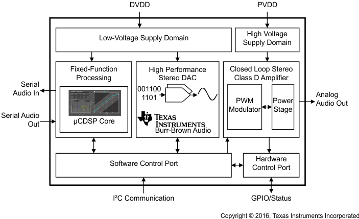
The TAS5780M device is a high-performance, stereo closed-loop Class-D amplifier with integrated audio processor with 96-kHz architecture. To convert from digital to analog, the device uses a high performance DAC with Burr Brown™ audio technology. It requires only two power supplies: one DVDD for low-voltage circuitry and one PVDD for high-voltage circuitry. It is controlled by a software control port using standard I2C communication.
An optimal mix of thermal performance and device cost is provided in the 90 mΩ rDS(on) of the output MOSFETs. Additionally, a thermally enhanced 48-Pin TSSOP provides excellent operation in the elevated ambient temperatures found in modern consumer electronic devices.
Device Information(1)
| PART NUMBER | PACKAGE | BODY SIZE (NOM) |
|---|---|---|
| TAS5780M | TSSOP (48) | 12.50 mm × 6.10 mm |
- For all available packages, see the orderable addendum at the end of the data sheet.
SPACE
Simplified Block Diagram

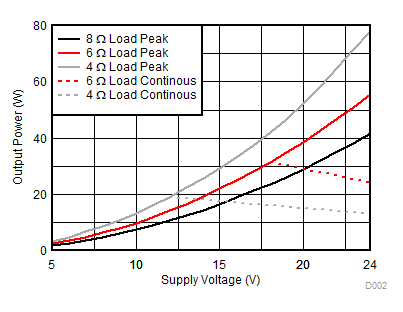
Power at 10% THD+N vs PVDD (1)
