SBOS908A November 2017 – December 2017 OPA2333P
PRODUCTION DATA.
- 1 Features
- 2 Applications
- 3 Description
- 4 Revision History
- 5 Pin Configuration and Functions
- 6 Specifications
- 7 Detailed Description
- 8 Application and Implementation
- 9 Power Supply Recommendations
- 10Layout
- 11Device and Documentation Support
- 12Mechanical, Packaging, and Orderable Information
Package Options
Mechanical Data (Package|Pins)
- DSG|8
Thermal pad, mechanical data (Package|Pins)
- DSG|8
Orderable Information
1 Features
2 Applications
- Smartphones
- Wearables
- Fitness and Healthcare Products
- Electronic Scales
- Medical Instrumentation
- Battery-Powered Instruments
- Handheld Test Equipment
- Circuit Breakers
3 Description
The OPA2333P is a CMOS operational amplifier that uses a proprietary auto-calibration technique to simultaneously provide very low offset voltage (10 μV, maximum) and near-zero drift over time and temperature. This miniature, high-precision, low quiescent current amplifier offers high-impedance inputs that have a common-mode range 100 mV beyond the rails, and rail-to-rail output that swings within 50 mV of the rails. Single or dual supplies as low as 1.8 V (±0.9 V) and up to 5.5 V (±2.75 V) can be used. This device is optimized for low-voltage, single-supply operation.
The OPA2333P also features a specified maximum start-up time. Specified start-up time ensures high-precision performance after 500 μs of powering the amplifier, allowing for reliable use in dynamic supply operation.
The OPA2333P offers excellent CMRR without the crossover associated with traditional complementary input stages. This design results in superior performance for driving analog-to-digital converters (ADCs) without degradation of differential linearity.
The OPA2333P is available in a 2-mm × 2-mm 8-pin WSON package and is specified for operation from –40°C to 125°C.
Device Information(1)
| PART NUMBER | PACKAGE | BODY SIZE (NOM) |
|---|---|---|
| OPA2333P | WSON (8) | 2.00 mm × 2.00 mm |
- For all available packages, see the orderable addendum at the end of the data sheet.
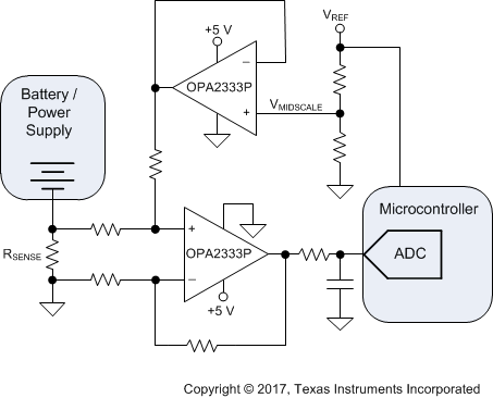
Bidirectional, Low-Side Current Shunt Amplifier

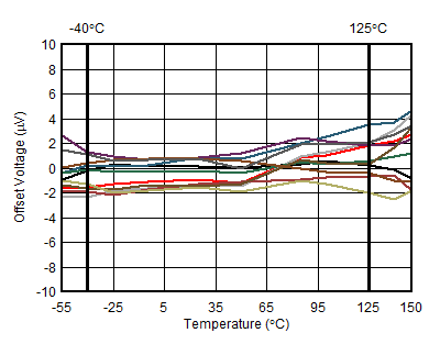
Offset Voltage vs Temperature
