SLLSEQ6A September 2016 – September 2016 ONET1131EC
PRODUCTION DATA.
- 1 Features
- 2 Applications
- 3 Description
- 4 Revision History
- 5 Pin Configuration and Function
- 6 Specifications
-
7 Detailed Description
- 7.1 Overview
- 7.2 Functional Block Diagram
- 7.3
Feature Description
- 7.3.1 Equalizer
- 7.3.2 CDR
- 7.3.3 Modulator Driver
- 7.3.4 Modulation Current Generator
- 7.3.5 DC Offset Cancellation and Cross Point Control
- 7.3.6 Bias Current Generation and APC Loop
- 7.3.7 Laser Safety Features and Fault Recovery Procedure
- 7.3.8 Analog Block
- 7.3.9 Acknowledge
- 7.4 Device Functional Modes
- 7.5 Programming
- 7.6
Register Mapping
- 7.6.1 R/W Control Registers
- 7.6.2
TX Registers
- 7.6.2.1 TX Register 10 (offset = 0000 0000) [reset = 0h]
- 7.6.2.2 TX Register 11 (offset = 0000 0000) [reset = 0h]
- 7.6.2.3 TX Register 12 (offset = 0000 0000) [reset = 0h]
- 7.6.2.4 TX Register 13 (offset = 0h) [reset = 0]
- 7.6.2.5 TX Register 14 (offset = 0000 0000) [reset = 0h]
- 7.6.2.6 TX Register 15 (offset = 0000 0000) [reset = 0h]
- 7.6.2.7 TX Register 16 (offset = 0000 0000) [reset = 0h]
- 7.6.2.8 TX Register 17 (offset = 0000 0000) [reset = 0h]
- 7.6.2.9 TX Register 18 (offset = 0000 0000) [reset = 0h]
- 7.6.2.10 TX Register 19 (offset = 0000 0000) [reset = 0h]
- 7.6.3 Reserved Registers
- 7.6.4 Read Only Registers
- 7.6.5 Adjustment Registers
- 8 Application Information and Implementations
- 9 Power Supply Recommendations
- 10Layout
- 11Device and Documentation Support
- 12Mechanical, Packaging, and Orderable Information
Package Options
Mechanical Data (Package|Pins)
- RSM|32
Thermal pad, mechanical data (Package|Pins)
- RSM|32
Orderable Information
1 Features
- Modulator Driver with Minimum Output Amplitude up to 2 Vpp Single-Ended and Bias Current up to 150 mA Source
- Supports Externally Modulated Lasers Including the Electro-Absorption Modulator Lasers (EML) and the Mach-Zahnder Modulator (MZM) Based lasers
- Integrated CDR with 9.80 – 11.7 Gbps Reference-Free Operation
- Two-Wire Digital Interface with Integrated DACs and ADC for Control and Diagnostic Management
- Output Polarity Select
- Programmable Jitter Transfer Bandwidth to Adjust CDR Bandwidth
- CDR Bypass Mode for Low Data Rate Operation
- Automatic Power Control (APC) Loop with Selectable Monitor PD Range
- Programmable Transmit Input Equalizer
- Transmitter Cross-Point Adjust and De-Emphasis
- Includes Laser Safety Features
- Power Supply Monitor and Temperature Sensor
- Single 2.5 V Supply
- –40°C to 100°C Operation
- Surface Mount 4 mm x 4 mm 32-Pin QFN Package with 0.4 mm Pitch
2 Applications
- 10-Gbps Passive Optical Network (PON), Optical Line Terminal (OLT) Transceivers for FTTx deployment
- XFP and SFP+ 10-Gbps SONET OC-192 Optical Transceivers
- XFP and SFP+ 10GBASE-ER/ZR Optical Transceivers
- 8x and 10x Fibre Channel Optical Transmitters
3 Description
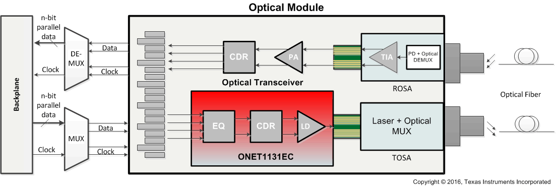
The ONET1131EC is a 2.5-V EML modulator driver with transmit clock and data recovery (CDR) designed to operate between 9.8 Gbps and 11.7 Gbps without the need for a reference clock. CDR bypass mode can be used for operation at lower data rates and a two-wire serial interface allows digital control of features like output polarity select and input equalization.
The transmit path consists of an adjustable input equalizer for equalization of up to 300 mm
(12 inches) of microstrip or stripline transmission line of FR4 printed circuit boards, a multi-rate CDR and an output modulator driver. Output waveform control, in the form of cross-point adjustment and de-emphasis, is available to improve the optical eye mask margin. The device provides bias current for the laser and an integrated automatic power control (APC) loop to compensate for variations in average optical power over voltage, temperature and time.
The ONET1131EC contains internal analog to digital and digital to analog converters to support transceiver management and eliminate the need for special purpose microcontrollers.
Device Information(1)
| PART NUMBER | PACKAGE | BODY SIZE (NOM) |
|---|---|---|
| ONET1131EC | VQFN (32) | 4.00 mm x 4.00 mm |
- For all available packages, see the orderable addendum at the end of the data sheet.
Simplified Block Diagram
