SNOS032I August 1999 – June 2016 LMV821-N , LMV822-N , LMV822-N-Q1 , LMV824-N , LMV824-N-Q1
PRODUCTION DATA.
- 1 Features
- 2 Applications
- 3 Description
- 4 Revision History
- 5 Pin Configuration and Functions
-
6 Specifications
- 6.1 Absolute Maximum Ratings
- 6.2 ESD Ratings
- 6.3 Recommended Operating Conditions
- 6.4 Thermal Information, 5 Pins
- 6.5 Thermal Information, 8 Pins
- 6.6 Thermal Information, 14 Pins
- 6.7 DC Electrical Characteristics 2.7V
- 6.8 DC Electrical Characteristics 2.5V
- 6.9 AC Electrical Characteristics 2.7V
- 6.10 DC Electrical Characteristics 5V
- 6.11 AC Electrical Characteristics 5V
- 6.12 Typical Characteristics
- 7 Detailed Description
- 8 Application and Implementation
- 9 Power Supply Recommendations
- 10Layout
- 11Device and Documentation Support
- 12Mechanical, Packaging, and Orderable Information
Package Options
Mechanical Data (Package|Pins)
Thermal pad, mechanical data (Package|Pins)
Orderable Information
1 Features
- Qualified for Automotive Applications
- AEC-Q100 Qualified With the Following Results:
- For Vs = 5 V, Typical Supply Values Unless Otherwise Noted
- LMV824 Available With Extended Temperature Range to 125°C
- Small SC70-5 Package 2.0 x 1.25 x 0.95 mm
- Specified Performance At 2.5 V, 2.7 V and 5 V
- VOS 3.5 mV (Max)
- TCVOS 1 uV/°C
- Gain Bandwidth Product At 2.7 V, 5 MHz
- ISupply At 2.7 V Supply, 220 μA per Amplifier
- Slew Rate 1.4 V/µs (Min)
- CMRR 90 dB
- PSRR 85 dB
- VCM At 5 V Supply, -0.3 V to 4.3 V
- Rail to Rail Output (RRO)
- 600 Ω Load, 160 mV From Rail
- 10 kΩ Load, 55 mV From Rail
- Stable Performance with Capacitive Loads
2 Applications
- Cordless Phones
- Cellular Phones
- Laptops
- PDAs
- PCMCIA
3 Description
The LMV821/LMV822/LMV824 op amps bring performance and economy to low voltage, low power systems. With a 5 MHz unity-gain frequency, at 2.7 V supply, and a 1.4 V/µs slew rate, the quiescent current is only 220 µA per amplifier. They provide rail to rail output (RRO) swing into 600 Ω load. The input common-mode voltage range includes ground and the maximum input offset voltage is 3.5 mV. They are also capable of easily driving large capacitive loads as indicated in the applications section.
The LMV821 single op amp is available in the tiny SC70-5 package, which is about half the size of the previous title holder, the SOT23-5. The LMV824NDGV is specified over the extended industrial temperature range and is in a TVSOP package.
Overall, the LMV821/LMV822/LMV824 devices are low voltage, low power and performance op amps designed for a wide range of applications at an economical price.
Device Information(1)
| DEVICE NAME | PACKAGE | BODY SIZE |
|---|---|---|
| LMV821-N | SOT23 (5) | 2.92 mm x 1.60 mm |
| SC70 (5) | 2.00 mm x 1.25 mm | |
| LMV822-N | SOIC (8) | 4.90 mm x 3.91 mm |
| VSSOP (8) | 3.00 mm x 3.00 mm | |
| LMV822-N-Q1 | VSSOP (8) | 3.00 mm x 3.00 mm |
| LMV824-N | SOIC (14) | 8.65 mm x 3.91 mm |
| TSSOP (14) | 5.00 mm x 4.40 mm | |
| LMV824-N-Q1 | TSSOP (14) | 5.00 mm x 4.40 mm |
| LMV824I | TVSOP (14) | 4.40 mm x 3.60 mm |
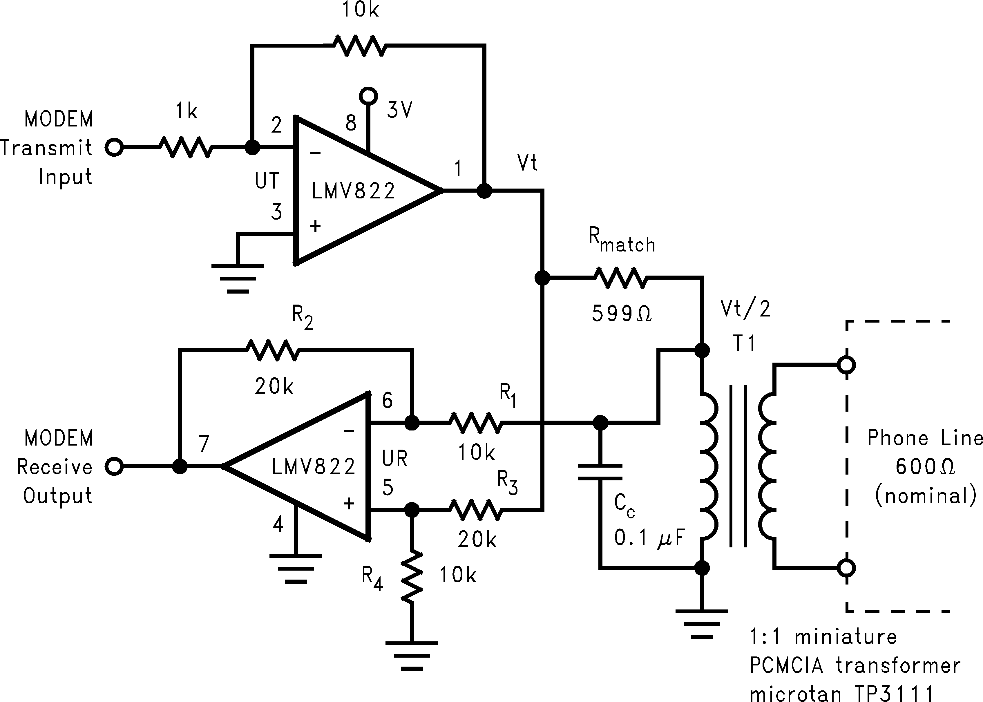
Telephone Line Transceiver for PCMCIA Modem Card
