SNVSAF0B December 2015 – May 2016 LM25122-Q1
PRODUCTION DATA.
- 1 Features
- 2 Applications
- 3 Description
- 4 Revision History
- 5 Pin Configuration and Functions
- 6 Specifications
-
7 Detailed Description
- 7.1 Overview
- 7.2 Functional Block Diagram
- 7.3
Feature Description
- 7.3.1 Undervoltage Lockout (UVLO)
- 7.3.2 High Voltage VCC Regulator
- 7.3.3 Oscillator
- 7.3.4 Slope Compensation
- 7.3.5 Error Amplifier
- 7.3.6 PWM Comparator
- 7.3.7 Soft-Start
- 7.3.8 HO and LO Drivers
- 7.3.9 Bypass Operation (VOUT = VIN)
- 7.3.10 Cycle-by-Cycle Current Limit
- 7.3.11 Clock Synchronization
- 7.3.12 Maximum Duty Cycle
- 7.3.13 Thermal Protection
- 7.4 Device Functional Modes
-
8 Application and Implementation
- 8.1 Application Information
- 8.2
Typical Application
- 8.2.1 Design Requirements
- 8.2.2
Detailed Design Procedure
- 8.2.2.1 Timing Resistor RT
- 8.2.2.2 UVLO Divider RUV2, RUV1
- 8.2.2.3 Input Inductor LIN
- 8.2.2.4 Current Sense Resistor RS
- 8.2.2.5 Current Sense Filter RCSFP, RCSFN, CCS
- 8.2.2.6 Slope Compensation Resistor RSLOPE
- 8.2.2.7 Output Capacitor COUT
- 8.2.2.8 Input Capacitor CIN
- 8.2.2.9 VIN Filter RVIN, CVIN
- 8.2.2.10 Bootstrap Capacitor CBST and Boost Diode DBST
- 8.2.2.11 VCC Capacitor CVCC
- 8.2.2.12 Output Voltage Divider RFB1, RFB2
- 8.2.2.13 Soft-Start Capacitor CSS
- 8.2.2.14 Restart Capacitor CRES
- 8.2.2.15 Low-Side Power Switch QL
- 8.2.2.16 High-Side Power Switch QH and Additional Parallel Schottky Diode
- 8.2.2.17 Snubber Components
- 8.2.2.18 Loop Compensation Components CCOMP, RCOMP, CHF
- 8.2.3 Application Curves
- 9 Power Supply Recommendations
- 10Layout
- 11Device and Documentation Support
- 12Mechanical, Packaging, and Orderable Information
Package Options
Mechanical Data (Package|Pins)
- PWP|20
Thermal pad, mechanical data (Package|Pins)
- PWP|20
Orderable Information
1 Features
-
AEC-Q100 Qualified with the following results:
- Device Temperature Grade 1: -40°C to +125°C Ambient Operating Temperature Range
- Device HBM ESD Classification Level 2
- Device CDM ESD Classification Level C6
- Maximum Input Voltage : 42 V
- Min Input Voltage : 3 V (4.5 V for startup)
- Output Voltage up to 50 V
- Bypass (VOUT = VIN) Operation
- 1.2 V Reference with ±1.0% Accuracy
- Free-Run and Synchronizable Switching to 600 kHz
- Peak Current Mode Control
- Robust 3 A Integrated Gate Drivers
- Adaptive Dead-Time Control
- Optional Diode Emulation Mode
- Programmable Cycle-by-Cycle Current Limit
- Hiccup Mode Overload Protection
- Programmable Line UVLO
- Programmable Soft-Start
- Thermal Shutdown Protection
- Low Shutdown Quiescent Current: 9 μA
- Programmable Slope Compensation
- Programmable Skip Cycle Mode Reduces Standby Power
- Allows External VCC Supply
- Inductor DCR Current Sensing Capability
- Multiphase Capability
- Thermally Enhanced 20-Pin HTSSOP
2 Applications
- 12-V, 24-V, and 48-V Power Systems
- Automotive Start-Stop
- Audio Power Supply
- High Current Boost Power Supply
3 Description
The LM25122 is a multiphase capable synchronous boost controller intended for high-efficiency synchronous boost regulator applications. The control method is based upon peak current mode control. Current mode control provides inherent line feed-forward, cycle-by-cycle current limiting and ease of loop compensation.
The switching frequency is programmable up to 600 kHz. Higher efficiency is achieved by two robust N-channel MOSFET gate drivers with adaptive dead-time control. A user-selectable diode emulation mode also enables discontinuous mode operation for improved efficiency at light load conditions.
An internal charge pump allows 100% duty cycle for high-side synchronous switch (Bypass operation). A 180º phase shifted clock output enables easy multi-phase interleaved configuration. Additional features include thermal shutdown, frequency synchronization, hiccup mode current limit and adjustable line undervoltage lockout.
Device Information(1)
| PART NUMBER | PACKAGE | BODY SIZE (NOM) |
|---|---|---|
| LM25122-Q1 | HTSSOP (20) | 6.50 mm × 4.40 mm |
- For all available packages, see the orderable addendum at the end of the data sheet.
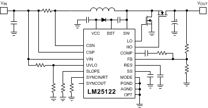
Simplified Application Diagram
