SNOSD15B December 2016 – April 2017 LDC2112 , LDC2114
PRODUCTION DATA.
- 1 Features
- 2 Applications
- 3 Description
- 4 Revision History
- 5 Pin Configuration and Functions
- 6 Specifications
-
7 Detailed Description
- 7.1 Overview
- 7.2 Functional Block Diagram
- 7.3 Feature Description
- 7.4 Device Functional Modes
- 7.5 Register Maps
-
8 Application and Implementation
- 8.1
Application Information
- 8.1.1 Theory of Operation
- 8.1.2 Designing Sensor Parameters
- 8.1.3 Setting COM Pin Capacitor
- 8.1.4 Defining Power-On Timing
- 8.1.5 Configuring Button Scan Rate
- 8.1.6 Programming Button Sampling Window
- 8.1.7 Scaling Frequency Counter Output
- 8.1.8 Setting Button Triggering Threshold
- 8.1.9 Tracking Baseline
- 8.1.10 Mitigating False Button Detections
- 8.1.11 Reporting Interrupts for Button Presses and Error Conditions
- 8.1.12 Estimating Supply Current
- 8.2 Typical Application
- 8.1
Application Information
- 9 Power Supply Recommendations
- 10Layout
- 11Device and Documentation Support
- 12Mechanical, Packaging, and Orderable Information
Package Options
Mechanical Data (Package|Pins)
Thermal pad, mechanical data (Package|Pins)
Orderable Information
1 Features
- Low Power Consumption:
- One Button: 6 µA at 0.625 SPS
- Two Buttons: 72 µA at 20 SPS
- Configurable Button Scan Rates:
- 0.625 SPS to 80 SPS
- Force Level Measurement of Touch Buttons
- Independent Channel Operation:
- Two Channels for LDC2112
- Four Channels for LDC2114
- Integrated Algorithms to Enable:
- Adjustable Force Threshold per Button
- Environmental Shift Compensation
- Simultaneous Button Press Detection
- Supports Independent Operation without MCU
- Robust EMI Performance:
- Allows for CISPR 22 and CISPR 24 Compliance
- Operating Voltage Range: 1.8 V ± 5%
- Temperature Range: –40 °C to +85 °C
- Interface:
- I2C
- Dedicated Logic Output per Channel
2 Applications
- Consumer Electronics:
- Smartphones
- Smart Watches and Other Wearable Devices
- Smart Speakers
- Tablets/PCs
- Virtual Reality Headsets
- Sound Bars
- Industrial Applications:
- Televisions
- Handheld Devices
- Home Appliances
- HMI Panels and Keypads
Touch Buttons and Force Level Measurements on Different Materials, Including Metal, Plastic, and Glass for:
3 Description
Inductive sensing technology enables touch button design for human machine interface (HMI) on a wide variety of materials such as metal, glass, plastic, and wood, by measuring small deflections of conductive targets. The sensor for an inductive touch system is a coil that can be implemented on a small PCB located behind the panel and protected from the environment. Inductive sensing solution is insensitive to humidity or non-conductive contaminants such as oil and dirt. It is able to automatically correct for any deformation in the conductive targets.
The LDC2112/LDC2114 is a multi-channel low-noise inductance to digital converter with integrated algorithms to implement inductive touch applications. The device employs an innovative LC resonator that offers high rejection of noise and interference. The LDC2112/LDC2114 can reliably detect material deflections of less than 200 nm.
The LDC2112/LDC2114 includes an ultra-low power mode intended for power on/off buttons in battery powered applications.
The LDC2112/LDC2114 is available in a 16-pin DSBGA or TSSOP package. The 0.4 mm pitch DSBGA package has a very small 1.6 × 1.6 mm nominal body size with a maximum height of 0.4 mm. The 0.65 mm pitch TSSOP package has a 5.0 × 4.4 mm nominal body size with a maximum height of 1.2 mm.
Device Information(1)
| PART NUMBER | PACKAGE | BODY SIZE (NOM) |
|---|---|---|
| LDC2112/LDC2114 | DSBGA (16) | 1.6 mm × 1.6 mm |
| LDC2112/LDC2114 | TSSOP (16) | 5.0 mm × 4.4 mm |
- For all available packages, see the orderable addendum at the end of the data sheet.
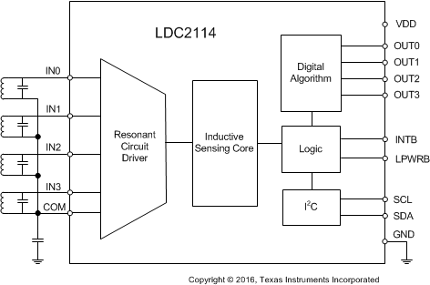
Simplified Schematic
