SLLSET5A March 2016 – September 2016 ISO7821LLS
PRODUCTION DATA.
- 1 Features
- 2 Applications
- 3 Description
- 4 Revision History
- 5 Pin Configuration and Functions
-
6 Specifications
- 6.1 Absolute Maximum Ratings
- 6.2 ESD Ratings
- 6.3 Recommended Operating Conditions
- 6.4 Thermal Information
- 6.5 Power Ratings
- 6.6 Insulation Specifications
- 6.7 Safety-Related Certifications
- 6.8 Safety Limiting Values
- 6.9 DC Electrical Characteristics
- 6.10 DC Supply Current Characteristics
- 6.11 Timing Requirements for Distortion Correction Scheme
- 6.12 Switching Characteristics
- 6.13 Insulation Characteristics Curves
- 6.14 Typical Characteristics
- 7 Parameter Measurement Information
- 8 Detailed Description
- 9 Application and Implementation
- 10Power Supply Recommendations
- 11Layout
- 12Device and Documentation Support
- 13Mechanical, Packaging, and Orderable Information
Package Options
Mechanical Data (Package|Pins)
Thermal pad, mechanical data (Package|Pins)
Orderable Information
1 Features
- Complies with TIA/EIA-644-A LVDS Standard
- Signaling Rate: 50 Mbps to 150 Mbps
- Optimized for DC-Balanced Data
- Wide Supply Range: 3 V to 5.5 V
- Wide Temperature Range: –55°C to 125°C
- Low-Power Consumption, Typical 10.3 mA per Channel at 150 Mbps
- Low Propagation Delay: 17 ns Typical
- Industry leading CMTI(Min): ±100 kV/μs
- Robust Electromagnetic Compatibility (EMC)
- System-Level ESD, EFT, and Surge Immunity
- Low Emissions
- Isolation Barrier Life: > 40 Years
- SOIC-16 Wide Body (DW) and Extra-Wide Body (DWW) Package Options
- Isolation Surge Withstand Voltage 12800 VPK
- Safety-Related Certifications:
- 8000-VPK Reinforced Isolation per DIN V VDE V 0884–10 (VDE V 0884–10): 2006–12
- 5700-VRMS Isolation for 1 minute per UL 1577
- CSA Component Acceptance Notice 5A, IEC 60950–1 and IEC 60601–1 End Equipment Standards
- TUV Certification per EN 61010-1 and EN 60950-1
- CQC Certification per GB4943.1–2011
- All Certifications are Planned
2 Applications
- Motor Control
- Test and Measurement
- Industrial Automation
- Medical Equipment
- Communication Systems
3 Description
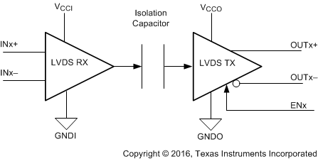
The ISO7821LLS device is a high-performance, isolated dual-LVDS buffer with 8000-VPK isolation voltage. This device provides high electromagnetic immunity and low emissions at low-power consumption, while isolating the LVDS bus signal. Each isolation channel has an LVDS receive and transmit buffer. Timing performance for the ISO7821LLS device is optimized for use with communication systems that use DC-balanced data streams which is achieved through an internal distortion correction scheme.
The ISO7821LLS device has one forward and one reverse-direction channel.
Through innovative chip design and layout techniques, the electromagnetic compatibility of the ISO7821LLS device has been significantly enhanced to ease system-level ESD, EFT, surge, and emissions compliance.
The ISO7821LLS device is available in a 16-pin SOIC wide-body (DW) and extra-wide body (DWW) packages.
Device Information(1)
| PART NUMBER | PACKAGE | BODY SIZE (NOM) |
|---|---|---|
| ISO7821LLS | DW (16) | 10.30 mm × 7.50 mm |
| DWW (16) | 10.30 mm × 14.00 mm |
- For all available packages, see the orderable addendum at the end of the data sheet.
Simplified Schematic
