SLVSCU7A February 2016 – March 2016 DRV10970
PRODUCTION DATA.
- 1 Features
- 2 Applications
- 3 Description
- 4 Revision History
- 5 Description (continued)
- 6 Pin Configuration and Functions
- 7 Specifications
- 8 Detailed Description
- 9 Application and Implementation
- 10Power Supply Recommendations
- 11Layout
- 12Device and Documentation Support
- 13Mechanical, Packaging, and Orderable Information
Package Options
Mechanical Data (Package|Pins)
- PWP|24
Thermal pad, mechanical data (Package|Pins)
- PWP|24
Orderable Information
1 Features
- Wide Power Supply Voltage Range: 5 to 18 V
- Integrated FETs: 1-A RMS, 1.5-A Peak Output Phase/Winding Current
- Total Driver H + L RDSON: 400 mΩ
- Embedded 180° Sine-Wave and Trapezoidal Commutations
- Ultra-Low Power Consumption in Sleep Mode
(35 µA) - Adaptive Drive Angle Adjustment
- Three or Single Hall Sensor Option to Minimize System Cost
- Motor Spin Direction Control
- Configurable for 30° Hall Placement or 0° Hall Placement
- Adjustable Retry Timing after Motor Lock
- Programmable Current-Limit Function
- Tachometer – Motor Speed Information on Open-Drain FG Pin
- Motor Lock Report on Open-Drain RD Pin
- Protection Features
- Supply (VM) Undervoltage Lockout
- Cycle-by-Cycle Current Limit
- Overcurrent Protection (OCP)
- Thermal Shutdown
- Motor Lock Detect and Report
2 Applications
- Cooling Fans
- Small Appliances
- General-Purpose BLDC Motor Driver
3 Description
The DRV10970 is an integrated three-phase BLDC motor driver for home appliance, cooling fans, and other general-purpose motor control applications. The embedded intelligence, small form factor, and simple pinout structure reduce the design complexity, board space, and system cost. The integrated protections improve the system robustness and reliability.
The output stage of DRV10970 consists of three half-bridges with RDSON of 400 mΩ (H + L). Each half-bridge is capable of driving up to 1-A RMS and 1.5-A peak output current. When the device enters sleep mode, it consumes typical 35 µA of current.
The advanced 180° sine-wave commutation algorithm is embedded into the device and achieves high efficiency, low torque ripple, and superior acoustic performance. The adaptive driving angle adjustment function achieves the most optimized efficiency regardless of the motor parameters and load conditions.
The DRV10970 is designed for either differential or single-ended Hall sensor based applications. The differential Hall signal inputs are detected by the integrated comparators. The device supports three Hall and single Hall based applications; the single Hall sensor mode reduces the system cost by eliminating two Hall sensors.
Device Information(1)
| PART NUMBER | PACKAGE | BODY SIZE (NOM) |
|---|---|---|
| DRV10970 | TSSOP (24) | 7.80 mm × 6.40 mm |
- For all available packages, see the orderable addendum at the end of the data sheet.
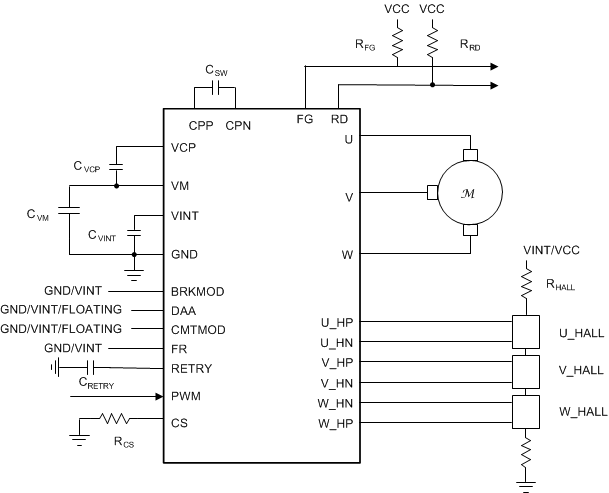
Application Circuit

4 Revision History
Changes from * Revision (February 2016) to A Revision
- Changed device status to Production Data and released full datasheetGo