SWRS154B October 2013 – October 2014 CC1201
PRODUCTION DATA.
- 1 Device Overview
- 2Revision History
- 3Terminal Configuration and Functions
-
4Specifications
- 4.1 Absolute Maximum Ratings
- 4.2 Handling Ratings
- 4.3 Recommended Operating Conditions (General Characteristics)
- 4.4 Thermal Resistance Characteristics for RHB Package
- 4.5 RF Characteristics
- 4.6 Regulatory Standards
- 4.7 Current Consumption, Static Modes
- 4.8 Current Consumption, Transmit Modes
- 4.9 Current Consumption, Receive Modes
- 4.10
Receive Parameters
- 4.10.1 General Receive Parameters (High-Performance Mode)
- 4.10.2 RX Performance in 868-, 915-, and 920-MHz Bands (High-Performance Mode)
- 4.10.3 RX Performance in 433-MHz Band (High-Performance Mode)
- 4.10.4 RX Performance in 169-MHz Band (High-Performance Mode)
- 4.10.5 RX Performance in Low-Power Mode
- 4.11 Transmit Parameters
- 4.12 PLL Parameters
- 4.13 Wake-up and Timing
- 4.14 40-MHz Crystal Oscillator
- 4.15 40-MHz Clock Input (TCXO)data to TCXO table
- 4.16 32-kHz Clock Input
- 4.17 40-kHz RC Oscillator
- 4.18 I/O and Reset
- 4.19 Temperature Sensor
- 4.20 Typical Characteristics
- 5Detailed Description
- 6Typical Application Circuit
- 7Device and Documentation Support
- 8Mechanical Packaging and Orderable Information
Package Options
Refer to the PDF data sheet for device specific package drawings
Mechanical Data (Package|Pins)
- RHB|32
Thermal pad, mechanical data (Package|Pins)
- RHB|32
Orderable Information
1 Device Overview
1.1 Features
- RF Performance and Analog Features:
- High-Performance, Single-Chip Transceiver
- Excellent Receiver Sensitivity:
- –120 dBm at 1.2 kbps
- –109 dBm at 50 kbps
- Blocking Performance: 85 dB at 10 MHz
- Adjacent Channel Selectivity: Up to 62 dB at 50-kHz Offset
- Very Low Phase Noise: –114 dBc/Hz at
10-kHz Offset (169 MHz)
- Excellent Receiver Sensitivity:
- Programmable Output Power Up to +16 dBm With 0.4-dB Step Size
- Automatic Output Power Ramping
- Supported Modulation Formats:
2-FSK, 2-GFSK, 4-FSK, 4-GFSK, MSK, OOK - Supports Data Rate Up to 1.25 Mbps in Transmit and Receive
- High-Performance, Single-Chip Transceiver
- Low Current Consumption:
- Enhanced Wake-On-Radio (eWOR) Functionality for Automatic Low-Power Receive Polling
- Power Down: 0.12 μA (0.5 μA With eWOR Timer Active)
- RX: 0.5 mA in RX Sniff Mode
- RX: 19 mA Peak Current in Low-Power Mode
- RX: 23 mA Peak Current in High-Performance Mode
- TX: 46 mA at +14 dBm
- Other:
- Data FIFOs: Separate 128-Byte RX and TX
- Support for Seamless Integration With the CC1190 Device for Increased Range Providing up to 3-dB Improvement in RX Sensitivity and up to +27 dBm TX Output Power
- Digital Features:
- WaveMatch: Advanced Digital Signal Processing for Improved Sync Detect Performance
- Autonomous Image Removal
- Security: Hardware AES128 Accelerator
- Data FIFOs: Separate 128-Byte RX and TX
- Includes Functions for Antenna Diversity Support
- Support for Retransmission
- Support for Auto-Acknowledge of Received Packets
- Automatic Clear Channel Assessment (CCA) for Listen-Before-Talk (LBT) Systems
- Built-in Coding Gain Support for Increased Range and Robustness
- Digital RSSI Measurement
- Improved OOK Shaping for Less Occupied Bandwidth, Enabling Higher Output Power While Meeting Regulatory Requirements
- Dedicated Packet Handling for 802.15.4g:
- CRC 16/32
- FEC, Dual Sync Detection (FEC and non-FEC Packets)
- Whitening
- General:
- RoHS-Compliant 5-mm × 5-mm No-Lead QFN 32-Pin Package (RHB)
- Pin-Compatible With the CC1120 Device
- Regulations – Suitable for Systems Targeting Compliance With:
- Europe: ETSI EN 300 220
- US: FCC CFR47 Part 15
- Japan: ARIB STD-T108
1.2 Applications
- Low-Power, High-Performance, Wireless Systems With Data Rate up to 1250 kbps
- ISM/SRD Bands: 169, 433, 868, 915, and
920 MHz - Possible Support for Additional Frequency Bands: 137 to 158.3 MHz, 205 to 237.5 MHz, and 274 to 316.6 MHz
- Smart Metering (AMR/AMI)
- Home and Building Automation
- Wireless Alarm and Security Systems
- Industrial Monitoring and Control
- Wireless Healthcare Applications
- Wireless Sensor Networks and Active RFID
- IEEE 802.15.4g Applications
1.3 Description
The CC1201 device is a fully integrated single-chip radio transceiver designed for high performance at very low-power and low-voltage operation in cost-effective wireless systems. All filters are integrated, thus removing the need for costly external SAW and IF filters. The device is mainly intended for the ISM (Industrial, Scientific, and Medical) and SRD (Short Range Device) frequency bands at 164–190 MHz, 410–475 MHz, and 820–950 MHz.
The CC1201 device provides extensive hardware support for packet handling, data buffering, burst transmissions, clear channel assessment, link quality indication, and Wake-On-Radio. The main operating parameters of the CC1201 device can be controlled through an SPI interface. In a typical system, the CC1201 device will be used with a microcontroller and only few external passive components.
The CC1201 offers the same performance as the CC1200 for channel filter bandwidths of 50 kHz or more, and therefore presents a lower cost option for applications that do not require narrowband support.
1.4 Functional Block Diagram
Figure 1-1 shows the system block diagram of the CC120x family of devices.
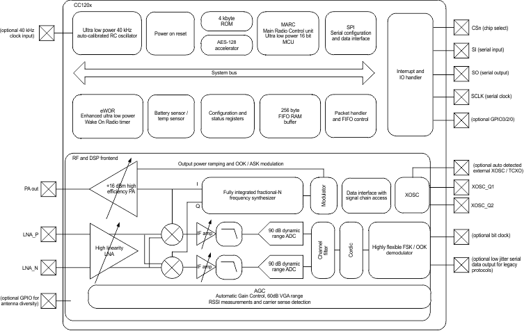 Figure 1-1 System Block Diagram