SLUS871D January 2009 – December 2016 UC1846-SP
PRODUCTION DATA.
- 1 Features
- 2 Applications
- 3 Description
- 4 Revision History
- 5 Pin Configuration and Functions
- 6 Specifications
- 7 Detailed Description
- 8 Application and Implementation
- 9 Power Supply Recommendations
- 10Layout
- 11Device and Documentation Support
- 12Mechanical, Packaging, and Orderable Information
封装选项
机械数据 (封装 | 引脚)
散热焊盘机械数据 (封装 | 引脚)
订购信息
10 Layout
10.1 Layout Guidelines
Always try to use a low EMI inductor with a ferrite type closed core. Some examples would be toroid and encased E core inductors. Open core can be used if they have low EMI characteristics and are located a bit more away from the low power traces and components. Make the poles perpendicular to the PCB as well if using an open core. Stick cores usually emit the most unwanted noise.
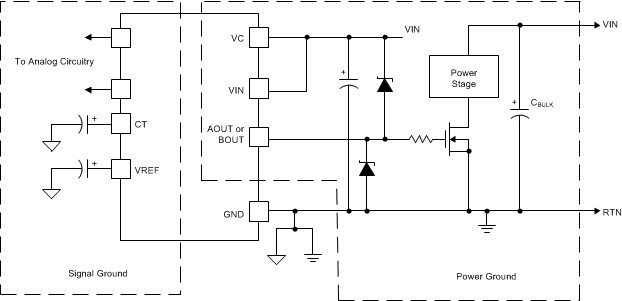
Each output driver of these devices is capable of 2-A peak currents. Careful layout is essential for correct operation of the chip. A ground plane must be employed. A unique section of the ground plane must be designated for high di/dt currents associated with the output stages. Power ground can be separated from the rest of the ground plane and connected at a single point, although this is not necessary if the high di/dt paths are well understood and accounted for. VIN should be bypassed directly to power ground with a good high frequency capacitor. The sources of the power MOSFET should connect to power ground as should the return connection for input power to the system and the bulk input capacitor. The output should be clamped with a high current Schottky diode to both VIN and GND. Nothing else should be connected to power ground.
VREF should be bypassed directly to the signal portion of the ground plane with a good high frequency capacitor. Low ESR/ESL ceramic 1-μF capacitors are recommended for both VIN and VREF. All analog circuitry should likewise be bypassed to the signal ground plane.
10.2 Layout Example
 Figure 16. Layout Recommendation