SLUS871D January 2009 – December 2016 UC1846-SP
PRODUCTION DATA.
- 1 Features
- 2 Applications
- 3 Description
- 4 Revision History
- 5 Pin Configuration and Functions
- 6 Specifications
- 7 Detailed Description
- 8 Application and Implementation
- 9 Power Supply Recommendations
- 10Layout
- 11Device and Documentation Support
- 12Mechanical, Packaging, and Orderable Information
封装选项
机械数据 (封装 | 引脚)
散热焊盘机械数据 (封装 | 引脚)
订购信息
7 Detailed Description
7.1 Overview
The UC1846-SP control devices provide all of the necessary features to implement fixed frequency, current mode control schemes while maintaining a minimum external parts count. The superior performance of this technique can be measured in improved line regulation, enhanced load response characteristics, and a simpler, easier-to-design control loop. Topological advantages include inherent pulse-by-pulse current limiting capability, automatic symmetry correction for push-pull converters, and the ability to parallel “power modules" while maintaining equal current sharing.
7.2 Functional Block Diagram
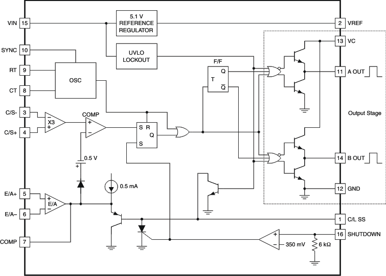
NOTE:
Pin numbers shown are for the J package.7.3 Feature Description
UC1846-SP is a current mode controller, used to support various topologies such as forward, flyback, half-bridge, full bridge, push-pull configurations.
Current mode control is a two-loop system. The switching power supply inductor is hidden within the inner current control loop. This simplifies the design of the outer voltage control loop and improves power supply performance in many ways, including better dynamics. The objective of this inner loop is to control the state-space averaged inductor current, but in practice the instantaneous peak inductor current is the basis for control (switch current, equal to inductor current during the on time, is often sensed). If the inductor ripple current is small, peak inductor current control is nearly equivalent to average inductor current control.
The peak method of inductor current control functions by comparing the upslope of inductor current (or switch current) to a current program level set by the outer loop. The comparator turns the power switch off when the instantaneous current reaches the desired level. The current ramp is usually quite small compared to the programming level, especially when VIN is low. As a result, this method is extremely susceptible to noise. A noise spike is generated each time the switch turns on. A fraction of a volt coupled into the control circuit can cause it to turn off immediately, resulting in a sub-harmonic operating mode with much greater ripple. Circuit layout and bypassing are critically important to successful operation.
The peak current mode control method is inherently unstable at duty ratios exceeding 0.5, resulting in sub-harmonic oscillation. A compensating ramp (with slope equal to the inductor current downslope) is usually applied to the comparator input to eliminate this instability. A slope compensation must be added to the sensed current waveform or subtracted from the control voltage to ensure stability above a 50% duty cycle. A compensating ramp (with slope equal to the inductor current downslope) is usually applied to the comparator input to eliminate this instability.
The pulse width modulator (PWM) of UC1846-SP is limited to a maximum duty cycle of 50%, thus it can be used in topologies such as push-pull, half bridge, full bridge, forward, flyback configurations. Limiting PWM to 50% duty cycle ensures that for isolated or transformer based topologies. The transformer is allowed to reset and prevent saturation of the transformer core.
Pulse-by-pulse symmetry correction (flux balancing) is inherent to current mode controllers and essential for the push-pull topology to prevent core saturation.
Current limit control design has numerous advantages:
- Current mode control provided peak switch current limiting – pulse by pulse current limit.
- Control loop is simplified as one pole due to output inductor is pushed to higher frequency , thus a two pole system turns into two real poles. Thus system reduces to a first order system thus simplifies the control.
- Multiple converter can be paralleled and allows equal current sharing amount the various converters.
- Inherently provides for input voltage feed-forward as any perturbation in the input voltage will be reflected in the switch or inductor current. Since switch or inductor current is a direct control input, thus this perturbation is very rapidly corrected.
- The error amplifier output (outer control loop) defines the level at which the primary current (inner loop) will regulate the pulse width, and output voltage.
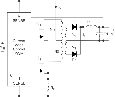 Figure 3. Push-Pull Converter Using Current Mode Control
7.3.1 Reference
As highlighted in the Functional Block Diagram, UC1846-SP incorporates a 5.1-V internal reference regulator with ±10% set point variation over temperature.
7.3.2 Oscillator
Figure 8 highlights the oscillator circuit. Connecting a resistor RT from pin 9 to ground establishes a current, which is mirrored to pin 8 and charges the capacitor connected from pin 8 to ground. Maximum on time corresponds to the maximum charging time of the timing capacitor. Oscillator frequency can be determined by .
Off-time corresponds to capacitor discharge time establishes the converter dead time between the pulses according to . Internal 8-mA current sink discharges the CT pin capacitor.
7.3.3 Slope Compensation
For duty cycle above 50% slope compensating can be implemented by using a buffer (that is, 2N2222) and connecting base to timing capacitor pin 8, collector to VREF (5 V), a resistor in series with emitter connected to (pin 4) CS+ of differential current sense amplifier. Injecting a downslope proportional to the sawtooth into current sense amplifier.
As with any bipolar PWM IC, outputs should be protected from negatively biasing the substrate. This is typically done by using Schottky diodes from ground to each output. Failure to do this could cause spurious interruption and restart of the oscillator, dropping of output pulses and a significant increase in propagation delays.
7.3.4 Error Amplifier
UC1846-SP incorporates an error amplifier with typical open loop gain of 100 dB and gain bandwidth of 1.5 MHz. With Source and sink capability of 10 mA and 0.5 mA respectively.
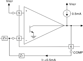
7.3.5 Current Sense Amplifier
UC1846-SP incorporates a differential current sense amplifier which can eliminate ground loop problems and increase noise immunity. An R-C snubber can also be implemented thus helping in blanking the peak current spike when the switch is turned on. The input of the current sense amplifier is slew rate limited allowing lower values of filter capacitors to be used to eliminate leading edge noise.

In some applications, a small RC filter is required to reduce switch transients. Differential input allows remote noise sensing.
7.3.6 Current Limit
Over current trip point is determined by Equation 1. Differential current sense amplifier has a gain of three, as shown in Figure 6.
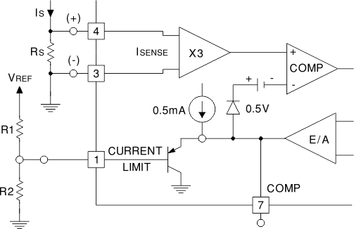 Figure 6. Pulse-By-Pulse Current Limiting
Referring to Figure 6, Equation 1 determines the peak current, Is.

7.3.7 Shutdown
UC1846-SP incorporates a shutdown pin (pin 16). Shutdown threshold voltage is 350 mV. Exceeding the shutdown threshold voltage causes the device to shutdown.
- If current into ICL_SS VREF/R1 > 3-mA SCR holding current (minimum latch current), then the device latches off. Power recycle is required to un-latch the device.
- If VREF/R1 < 0.8 mA, that is ICL_SS < 0.8 A, then this ensures that the circuit does not latch in a shutdown state.
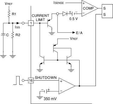 Figure 7. Shutdown Latch
Referring to Figure 11, if

the shutdown latch commutates when ISS = 0.8 mA and a restart cycle initiates.
Referring to Figure 12, if

the device latches off until power is recycled.
7.3.8 Output Section
UC1846-SP incorporates high current dual totem pole output stage capable of sourcing/sinking 1.5-A peak current for fast switching of power MOSFETs and limited to 0.5-A DC current.
7.3.9 Undervoltage Lockout
Minimum input voltage for converter is 8 V or higher, with typical value being 7.7 V. At input voltages below the actual UVLO voltage, the devices will not operate.
7.3.10 Soft-Start
Connecting a capacitor from CL/SS pin 1 to ground which is charged by 0.5-mA internal current source will determine the soft-start time. If over current is also implemented as shown in Figure 6, then SS charge time will be determined by charging SS capacitor by 0.5-mA current as well as current contributed by R1 resistor in charging the SS capacitor.
7.4 Device Functional Modes
7.4.1 Operation With VIN < 8 V (Minimum VIN)
The devices operate with input voltages above 8 V. The maximum UVLO voltage is 8 V and will operate at input voltages above 8 V. The typical UVLO voltage is 7.7 V and the devices may operate at input voltages above that point. The devices also may operate at lower input voltages, the minimum UVLO voltage is not specified. At input voltages below the actual UVLO voltage, the devices will not operate.
7.4.2 Synchronization
The synchronization pin (pin10) can be configured as an output for master/slave application. When the converter is configured as a master or standalone converter, SYNC (pin 10) is an output. As highlighted in the functional block diagram, voltage at RT (pin 9) is greater than 4.1-V internal threshold.
When using the part in slave configuration, SYNC pin becomes an input. Typical example of parallel operation with master/slave configuration is shown in Figure 13. Slave unit CT (pin 8) is grounded and RT pin is connected to VREF (pin 2).
When using the part in slave configuration, SYNC pin becomes an input. Typical example of parallel operation with master/slave configuration is shown in Figure 13. Slave unit CT (pin 8) is grounded and RT pin is connected to VREF (pin 2). Under parallel configuration two or more units can be paralleled, with COMP pins tied together each will share current equally.
7.4.3 Parallel Operation
Under parallel configuration two or more units can be paralleled, with COMP pins tied together each will share current equally.
Figure 13 highlights typical parallel operation configuration.