ZHCSGM7A August   2017  – September 2017 TUSB212

PRODUCTION DATA.  

  1. 特性
  2. 应用
  3. 说明
    1.     Device Images
      1.      简化的原理图
  4. 修订历史记录
  5. Pin Configuration and Functions
    1.     Pin Functions
  6. Specifications
    1. 6.1 Absolute Maximum Ratings
    2. 6.2 ESD Ratings
    3. 6.3 Recommended Operating Conditions
    4. 6.4 Thermal Information
    5. 6.5 Electrical Characteristics
    6. 6.6 Switching Characteristics
    7. 6.7 Typical Characteristics
  7. Detailed Description
    1. 7.1 Overview
    2. 7.2 Functional Block Diagram
    3. 7.3 Feature Description
      1. 7.3.1 EQ
      2. 7.3.2 DC BOOST
    4. 7.4 Device Functional Modes
      1. 7.4.1 Low Speed (LS) Mode
      2. 7.4.2 Full Speed (FS) Mode
      3. 7.4.3 High Speed (HS) Mode
      4. 7.4.4 Shutdown Mode
      5. 7.4.5 I2C Mode
  8. Application and Implementation
    1. 8.1 Application Information
    2. 8.2 Typical Application
      1. 8.2.1 Design Requirements
      2. 8.2.2 Detailed Design Procedure
        1. 8.2.2.1 Test Procedure to Construct USB High Speed Eye Diagram
          1. 8.2.2.1.1 For a Host Side Application
          2. 8.2.2.1.2 For a Device Side Application
      3. 8.2.3 Application Curves
  9. Power Supply Recommendations
  10. 10Layout
    1. 10.1 Layout Guidelines
    2. 10.2 Layout Example
  11. 11器件和文档支持
    1. 11.1 文档支持
    2. 11.2 接收文档更新通知
    3. 11.3 社区资源
    4. 11.4 商标
    5. 11.5 静电放电警告
    6. 11.6 Glossary
  12. 12机械、封装和可订购信息

封装选项

机械数据 (封装 | 引脚)
散热焊盘机械数据 (封装 | 引脚)
订购信息

Detailed Design Procedure

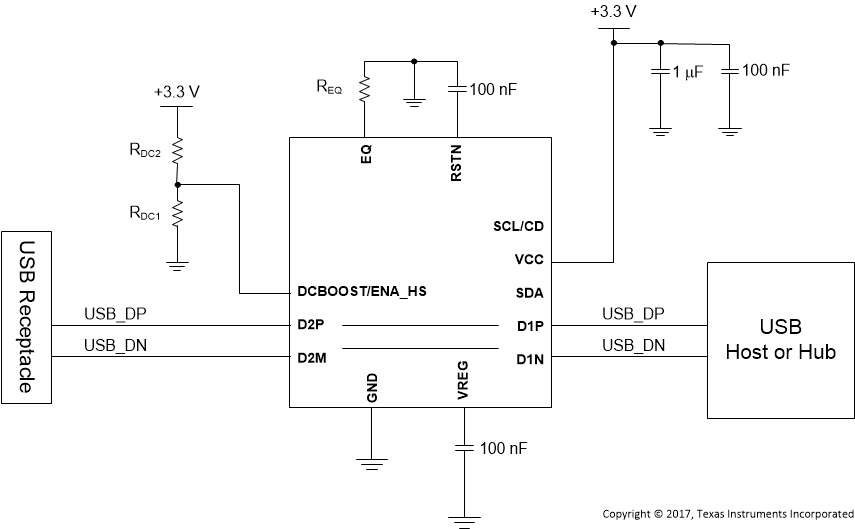
TUSB212 requires a valid reset signal as described in the power supply recommendations section. The capacitor at RSTN pin is not required if a microcontroller drives the RSTN pin according to recommendations.

VREG pin is the internal LDO output that requires a 0.1-μF external capacitor to GND to stabilize the core.

The ideal AC/DC Boost setting is dependent upon the signal chain loss characteristics of the target platform. The general recommendation is to start with AC Boost level 0, and then increment to AC Boost level 1, etc. when needed. Same applies to the DC boost setting where it is recommended to plan for the required pad to change boost settings.

In order for the TUSB212 to recognize any change to the AC or DC boost settings, the RSTN pin must be toggled. This is because the EQ and DC_BOOST pins are latched on power up and the pins are ignored thereafter.

Further D1P has to be shorted to D2P and D1M shorted to D2M on the board for correct functionality of the device.

Placement of the device is also dependent on the application goal. Table 4 summarizes our recommendations.

Table 4. Platform Placement Guideline

PLATFORM GOALSUGGESTED TUSB212 PLACEMENT
Pass USB Near End Mask Close to measurement point
Pass USB Far End Eye Mask Close to USB PHY
Cascade multiple TUSB212 to improve device enumeration Midway between each USB interconnect
TUSB212 SLLSEX5_Schematic.gif
D2P must be shorted to D1P on PCB.
D2N must be shorted to D1N on PCB.
Figure 7. Reference Schematic