ZHCSGM7A August   2017  – September 2017 TUSB212

PRODUCTION DATA.  

  1. 特性
  2. 应用
  3. 说明
    1.     Device Images
      1.      简化的原理图
  4. 修订历史记录
  5. Pin Configuration and Functions
    1.     Pin Functions
  6. Specifications
    1. 6.1 Absolute Maximum Ratings
    2. 6.2 ESD Ratings
    3. 6.3 Recommended Operating Conditions
    4. 6.4 Thermal Information
    5. 6.5 Electrical Characteristics
    6. 6.6 Switching Characteristics
    7. 6.7 Typical Characteristics
  7. Detailed Description
    1. 7.1 Overview
    2. 7.2 Functional Block Diagram
    3. 7.3 Feature Description
      1. 7.3.1 EQ
      2. 7.3.2 DC BOOST
    4. 7.4 Device Functional Modes
      1. 7.4.1 Low Speed (LS) Mode
      2. 7.4.2 Full Speed (FS) Mode
      3. 7.4.3 High Speed (HS) Mode
      4. 7.4.4 Shutdown Mode
      5. 7.4.5 I2C Mode
  8. Application and Implementation
    1. 8.1 Application Information
    2. 8.2 Typical Application
      1. 8.2.1 Design Requirements
      2. 8.2.2 Detailed Design Procedure
        1. 8.2.2.1 Test Procedure to Construct USB High Speed Eye Diagram
          1. 8.2.2.1.1 For a Host Side Application
          2. 8.2.2.1.2 For a Device Side Application
      3. 8.2.3 Application Curves
  9. Power Supply Recommendations
  10. 10Layout
    1. 10.1 Layout Guidelines
    2. 10.2 Layout Example
  11. 11器件和文档支持
    1. 11.1 文档支持
    2. 11.2 接收文档更新通知
    3. 11.3 社区资源
    4. 11.4 商标
    5. 11.5 静电放电警告
    6. 11.6 Glossary
  12. 12机械、封装和可订购信息

封装选项

机械数据 (封装 | 引脚)
散热焊盘机械数据 (封装 | 引脚)
订购信息

Switching Characteristics

over operating free-air temperature and voltage range (unless otherwise noted)
PARAMETERTEST CONDITIONSMINTYPMAXUNIT
FBR_DXX DxP/M bit rate USB channel = HS mode; 480 Mbps traffic; VCC supply stable 480.24 Mbps
tRISE_DXX DxP/M rise time 10% - 90%; VCC = 3.6V; Max AC Gain; 100 ps
tFALL_DXX DxP/M fall time 90% - 10%; VCC = 3.6V; Max AC Gain; 100 ps
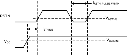
tRSTN_PULSE_WIDTH Minimum width to detect a valid RSTN signal assert when the pin is actively driven VCC = 3.0 V; Refer to Figure 1 20 µs
tSTABLE VCC stable before RSTN de-assertion  Refer to Figure 1 100 µs
tVCC_RAMP VCC ramp time 0.2 100 ms
TUSB212 timing-01-sllsex5.gifFigure 1. Power On and Reset Timing