ZHCSGS1A September   2017  – September 2017 TS5USBC400

PRODUCTION DATA.  

  1. 特性
  2. 应用
  3. 说明
    1.     Device Images
      1.      简化电路原理图
  4. 修订历史记录
  5. Pin Configuration and Functions
  6. Specifications
    1. 6.1 Absolute Maximum Ratings
    2. 6.2 ESD Ratings
    3. 6.3 Recommended Operating Conditions
    4. 6.4 Thermal Information
    5. 6.5 Electrical Characteristics
    6. 6.6 Dynamic Characteristics
    7. 6.7 Timing Requirements
    8. 6.8 Typical Characteristics
  7. Parameter Measurement Information
  8. Detailed Description
    1. 8.1 Overview
    2. 8.2 Functional Block Diagram
    3. 8.3 Feature Description
      1. 8.3.1 Powered-off Protection
      2. 8.3.2 Overvoltage Protection
    4. 8.4 Device Functional Modes
      1. 8.4.1 Pin Functions
  9. Application and Implementation
    1. 9.1 Application Information
    2. 9.2 Typical Application
      1. 9.2.1 Design Requirements
      2. 9.2.2 Detailed Design Procedure
      3. 9.2.3 Application Curves
  10. 10Power Supply Recommendations
  11. 11Layout
    1. 11.1 Layout Guidelines
    2. 11.2 Layout Example
  12. 12器件和文档支持
    1. 12.1 文档支持
      1. 12.1.1 相关文档
    2. 12.2 社区资源
    3. 12.3 商标
    4. 12.4 静电放电警告
    5. 12.5 Glossary
  13. 13机械、封装和可订购信息

封装选项

请参考 PDF 数据表获取器件具体的封装图。

机械数据 (封装 | 引脚)
  • YFP|12
散热焊盘机械数据 (封装 | 引脚)
订购信息

Overview

The TS5USBC400 is a bidirectional low-power dual port, high-speed, USB 2.0 analog switch with integrated protection for USB Type-C systems. The device is configured as a dual 2:1 or 1:2 switch and is optimized for handling the USB 2.0 D+/- lines in a USB Type-C system as shown in Figure 13.
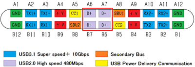
TS5USBC400 scds367_c_pinout.gifFigure 13. USB Type-C Connector Pinout

The TS5USBC400 also works in traditional USB systems that need protection from fault conditions such as automotive and applications that require higher voltage charging. The device maintains excellent signal integrity through the optimization of both RON and BW while protecting the system with 0 V to 16 V OVP protection. The OVP implementation is designed to protect sensitive system components behind the switch that cannot survive a fault condition where VBUS is shorted the D+ and D- pins on the connector.