SLUSCZ1 May 2017 TPS92518-Q1
PRODUCTION DATA.
- 1 Features
- 2 Applications
- 3 Description
- 4 Revision History
- 5 Pin Configuration and Functions
- 6 Specifications
- 7 Parameter Measurement Information
-
8 Detailed Description
- 8.1 Overview
- 8.2 Functional Block Diagram
- 8.3
Feature Description
- 8.3.1 General Operation
- 8.3.2 Important System Considerations: Off-Timer and Maximum Peak Threshold Values
- 8.3.3 Shunt FET or Matrix dimming: Maximum Off-timer Calculation
- 8.3.4 VIN and the VCC Internal Regulators
- 8.3.5 Output Enable Control Logic
- 8.3.6 BOOT Capacitor and BOOT UVLO
- 8.3.7 Drop-out Operation
- 8.3.8 Analog and PWM Dimming
- 8.3.9 VIN and CSPx Pin Configuration
- 8.3.10 Enable and Undervoltage Lock-out Configuration
- 8.3.11 Voltage Sampling and DAC Operation
- 8.3.12 Device Functional Modes
- 8.4 Serial Interface
- 8.5
Registers
- 8.5.1 CONTROL Register (Address = 00h) [reset = 00h]
- 8.5.2 STATUS (FAULT) Register (Address = 01h) [reset = 10h]
- 8.5.3 THERM_WARN_LMT Register (Address = 02h) [reset = 80h]
- 8.5.4 LED1_PKTH_DAC Register (Address = 03h) [reset = 80h]
- 8.5.5 LED2_PKTH_DAC Register (Address = 04h) [reset = 80h]
- 8.5.6 LED1_TOFF_DAC Register (Address = 05h) [reset = 80h]
- 8.5.7 LED2_TOFF_DAC Register (Address = 06h) [reset = 80h]
- 8.5.8 LED1_MAXOFF_DAC Register (Address = 07h) [reset = 80h]
- 8.5.9 LED2_MAXOFF_DAC Register (Address = 08h) [reset = 80h]
- 8.5.10 VTHERM Register (Address = 09h) [reset = 0h]
- 8.5.11 LED1_MOST_RECENT Register (Address = 0Ah) [reset = 0h]
- 8.5.12 LED1_LAST_ON Register (Address = 0Bh) [reset = 0h]
- 8.5.13 LED1_LAST_OFF Register (Address = 0Ch) [reset = 0h]
- 8.5.14 LED2_MOST_RECENT Register (Address = 0Dh) [reset = 0h]
- 8.5.15 LED2_LAST_ON Register (Address = 0Eh) [reset = 0h]
- 8.5.16 LED2_LAST_OFF Register (Address = 0Fh) [reset = 0h]
- 8.5.17 Reset Register (Address = 10h) [reset = 0h]
- 8.6 Programming
- 9 Application and Implementation
- 10Power Supply Recommendations
- 11Layout
- 12Device and Documentation Support
- 13Mechanical, Packaging, and Orderable Information
6 Specifications
6.1 Absolute Maximum Ratings
over operating free-air temperature range (unless otherwise noted)(1)| MIN | MAX | UNIT | |||
|---|---|---|---|---|---|
| VIN, EN/UV, CSPx, CSNx, SWx, VLEDx to GND | TPS92518HV-Q1 | –0.3 | 67 | V | |
| TPS92518-Q1 | -0.3 | 44 | |||
| MOSI, MISO, SCK, SSN to GND | –0.3 | 5.5 | |||
| PWMx, VCCx to GND | –0.3 | 8.8 | |||
| GATEx, BOOTx to SWx | –0.3 | 8.8 | |||
| GATEx, BOOTx to GND | TPS92518HV-Q1 | –0.3 | 75 | ||
| TPS92518-Q1 | -0.3 | 52 | |||
| CSPx to CSNx | –0.3 | 5.5 | |||
| SWx to GND, 10ns transient | –2 | ||||
| Junction temperature, TJ | –40 | 150 | °C | ||
| Storage temperature , Tstg | –65 | 165 | |||
(1) Stresses beyond those listed under Absolute Maximum Ratings may cause permanent damage to the device. These are stress ratings only, which do not imply functional operation of the device at these or any other conditions beyond those indicated under Recommended Operating Conditions. Exposure to absolute-maximum-rated conditions for extended periods may affect device reliability.
6.2 ESD Ratings
| VALUE | UNIT | |||
|---|---|---|---|---|
| V(ESD) | Electrostatic discharge | Human-body model (HBM), per AEC Q100-002(1) | ±2000 | V |
| Charged-device model (CDM), per V AEC Q100-011 | ±750 | |||
(1) AEC Q100-002 indicates that HBM stressing shall be in accordance with the ANSI/ESDA/JEDEC JS-001 specification.
6.3 Recommended Operating Conditions
over operating free-air temperature range (unless otherwise noted)| MIN | MAX | UNIT | |||
|---|---|---|---|---|---|
| VIN | Input Voltage | TPS92518HV-Q1 | 6.5 | 65 | V |
| TPS92518-Q1 | 6.5 | 42 | V | ||
| TA | Operating ambient temperature (1) | -40 | 125 | °C | |
| TJ | Operating junction temperature | -40 | 150 | °C | |
(1) The TPS92518-Q1 can operate at an ambient temperature of up to +125ºC as long as the junction temperature maximum of +150ºC is not exceeded.
6.4 Thermal Information
| THERMAL METRIC(1) | TPS92518-Q1 | UNIT | |
|---|---|---|---|
| PWP (HTSSOP) | |||
| 24 PINS | |||
| RθJA | Junction-to-ambient thermal resistance | 32.5 | °C/W |
| RθJC(top) | Junction-to-case (top) thermal resistance | 17.9 | °C/W |
| RθJB | Junction-to-board thermal resistance | 15.7 | °C/W |
| ψJT | Junction-to-top characterization parameter | 0.4 | °C/W |
| ψJB | Junction-to-board characterization parameter | 15.5 | °C/W |
| RθJC(bot) | Junction-to-case (bottom) thermal resistance | 1.8 | °C/W |
(1) For more information about traditional and new thermal metrics, see the Semiconductor and IC Package Thermal Metrics application report.
6.5 Electrical Characteristics
VVIN = 14 V, -40 °C ≤ TJ ≤ 150 °C, unless otherwise specified| PARAMETER | TEST CONDITIONS | MIN | TYP | MAX | UNIT | |
|---|---|---|---|---|---|---|
| VCCx, VIN | ||||||
| VCCx | VCCx Voltage | VVIN = 40 V or VVIN = 65 V, 0 A ≤ External Load ≤ 500 µA | 6.9 | 7.5 | 8.25 | V |
| VCCx2 | VCCx Voltage with External Load | External Load = 500 µA | 6.9 | 7.5 | 8.25 | V |
| VCCx_UVLO | VCCx undervoltage lockout | Falling threshold, VVIN = 10 V | 5.65 | 5.9 | 6.1 | V |
| VCCx_UVHYS | VCCx undervoltage lockout Hysteresis | 0.25 | V | |||
| IVCCx-LIM | VCCx regulator current limit | VCC shorted to GND. | 25 | 38 | 48 | mA |
| IVIN | Operating Current | Not Switching | 3 | 4 | mA | |
| VDO | LDO drop-out voltage | IVCC = 5 mA, VVIN = 5 V | 90 | 225 | mV | |
| Peak Current Comparator (CSPx, CSNx) | ||||||
| VCSTx | VCSPx-VCSNx peak current threshold | LEDx_PKTH_DAC = 255 | 245 | 255 | 265 | mV |
| LEDx_PKTH_DAC = 127 | 118.5 | 127 | 135.5 | mV | ||
| LEDx_PKTH_DAC = 10 | 10 | mV | ||||
| ICSN | CSN input bias current | 0.4 | 1.5 | µA | ||
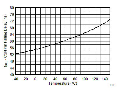
| tDEL | CSN pin falling delay | CSNx fall to GATEx fall (1V/us stimulus) | 58 | 110 | ns | |
| tLEB | Leading edge blanking (minimum on-time) | Minimum Pulse Width | 165 | 200 | 235 | ns |
| CSPUVLO | CSPx UVLO Falling Threshold | 4.65 | 4.90 | 5.15 | V | |
| CSPUVLO-H | CSPx UVLO Hysteresis | 520 | mV | |||
| Gate Drivers (GATEx, SWx and BOOTx) | ||||||
| RDSP | GATEx PFET ( RDS High ) | 7.3 | Ω | |||
| RDSN | GATEx NFET ( RDS Low ) | 2.8 | Ω | |||
| VBOOT-UVLO | Voltage where gate drive is disabled | VBOOT to VSW , VBOOT falling | 3.6 | 4.4 | 5.2 | V |
| VBOOT-UVLO-HYS | Hysteresis on BOOTx UVLO | VBOOTx to VSWx | 200 | mV | ||
| IPD PWMx | Pull down from SWx when PWMx Low | PWMx low, (BOOTx to SWx) = 5V, VSWx= 8V | 200 | 260 | µA | |
| IPD BOOTx | VBOOTx -VSWx < VBOOT-UVLO | PWMx high, (BOOTx to SWx) < BOOT_UVLO, VSWx = 8 V | 5 | 7 | mA | |
| IBOOT_Q | BOOTx quiescent current | (BOOTx to SWx) = 5.5 V, 0 V ≤ VSWx ≤ 65 V | 100 | 200 | µA | |
| OFF-TIMER | ||||||
| tOFF | Off-time | VLEDx = 30 V, tOFFXDAC = 255 | 3.2 | 4.1 | 4.8 | µs |
| tD-OFF | COFF threshold to gate rising delay | Specified by design | 50 | ns | ||
| tOFF-MAX | Maximum off-time | tOFF-MAXDAC = 255 | 65 | µs | ||
| Enable and Input UVLO | ||||||
| VEN/UV1 | EN/UV pin threshold | EN/UV pin rising | 1.18 | 1.24 | 1.30 | V |
| VEN/UV-HYS1 | EN/UV pin hysteresis | Difference between rising and falling threshold | 100 | mV | ||
| tEN/UV1 | EN/UV pin delay | EN/UV pin rising to GATEx pin rising. LEDx_MAXOFF_DAC = 0 | 300 | ns | ||
| EN/UV pin falling to GATEx pin falling | 470 | ns | ||||
| IEN/UV-HYST1 | EN/UV Hysteresis Current | EN/UV = 2 V | 12 | 16 | 28 | µA |
| VEN/UV2 | EN/UV LED1_EN and LED2_EN override threshold | EN/UV pin rising writes LED1_EN and LED2_EN = 1 | 23.4 | V | ||
| VEN/UV-HYS2 | EN/UV pin hysteresis | Difference between rising and falling threshold | 3 | V | ||
| tEN/UV2 | EN/UV pin delay 2 | EN/UV pin rising to GATEx pin rising. LEDx_MAXOFF_DAC = 0 | 520 | ns | ||
| PWM, MOSI, SCK, SSN | ||||||
| ILKG | Leakage current | 1 | µA | |||
| VIL | Low level input voltage threshold | 0.8 | V | |||
| VIH | High level input voltage threshold | 1.8 | V | |||
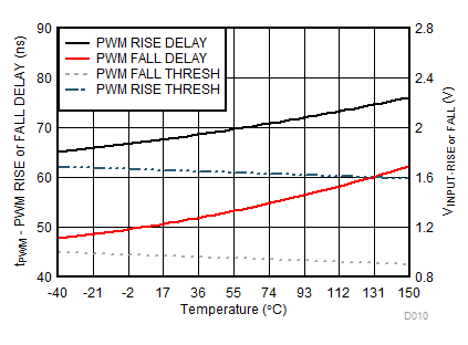
| tPWM | PWM pin delay | PWM pin rising to GATE pin rising | 68 | 105 | ns | |
| PWM pin falling to GATE pin falling | 55 | 100 | ns | |||
| MISO | ||||||
| VOL | MISO low, IMISO applied | IMISO = 10 mA | 0.26 | 0.51 | V | |
| RDS | MISO Pull-down resistance | IMISO = 10 mA | 26 | Ω | ||
| ADC | ||||||
| ADCTEMP | ADC Reading T = –40°C | 104 | Code | |||
| ADC Reading T = 25°C | 130 | Code | ||||
| ADC Reading T= 150°C | 171 | Code | ||||
| ADCLEDx | ADC Reading VLEDx= 60 V | 226 | 230 | 240 | Code | |
| ADC Reading VLEDx = 10 V | 37 | 38 | 39 | Code | ||
| ADC Reading VLEDx = 1 V | 2 | 3 | 4 | Code | ||
| SPI Interface | ||||||
| tSS_SU | SSN Setup Time | Falling edge of SSN to 1st SCK rising edge | 500 | ns | ||
| tSS_H | SSN Hold Time | Falling edge of 16th SCK to SSN rising edge | 250 | ns | ||
| tSCK | SCK Period | Clock period | 500 | ns | ||
| DSCK | SCK Duty Cycle | Clock duty cycle | 40 | 60 | % | |
| tSU | MOSI Setup Time | MOSI valid to rising edge SCK | 250 | ns | ||
| tH | MOSI Hold Time | MOSI valid after rising edge SCK | 275 | ns | ||
| tHI_Z | MISO Tri-State Time | Time to tri-state (deactivate low-side switch) MISO after SSN rising edge | 110 | 320 | ns | |
| tMISO_HL | MISO Valid High-to-Low | Time to place valid "0" on MISO after falling SCK edge | 320 | ns | ||
| tMISO_LH | MISO Valid Low-to-High | Time to tri-state (deactivate the internal low-side switch) MISO after falling SCK edge. tRC is the time added by the application total capacitance and resistance. | 320+tRC | ns | ||
| tZO_HL | MISO Drive Time High-to-Low | SSN Falling Edge to MISO Falling | 320 | ns | ||
| tSS | SSN High Time | How long SSN must remain high between transactions | 1000 | ns | ||
| THERMAL SHUTDOWN | ||||||
| TSD | Thermal shutdown temperature | 175 | °C | |||
| TSD HYST | Thermal shutdown hysteresis | 10 | ||||
6.6 Typical Characteristics
VVIN = 14 V unless otherwise specified. Temperature = Junction Temperature. Note: Any difference between channels does not necessarily illustrate a systematic difference between them.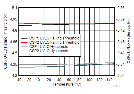
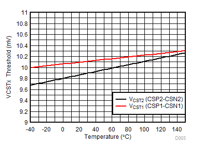
| VVIN = 42 V | LEDx_PKTH_DAC = 10 | |
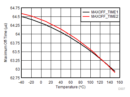
| LEDx_MAXOFF_DAC = 255 | ||
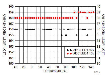
| Readings shown are TPS92518-Q1 register values |
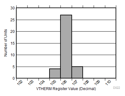
| TJ = -40°C |
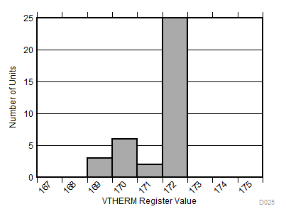
| TJ = 125°C |
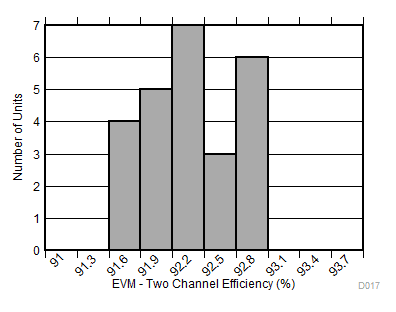
| 25 x TPS92518EVM-878 EVM's Tested | VVIN= VCSPx= 50 V | 22.3 V <= VVLED1= VVLED2 <= 25.1 V |
| LEDx_PKTH_DAC = 88 | LEDx_TOFF_DAC=70 | ILED1= ILED2 = 425 mA |
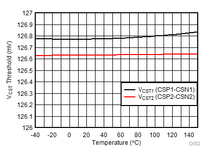
| VVIN = 42 V | LEDx_PKTH_DAC = 127 | |
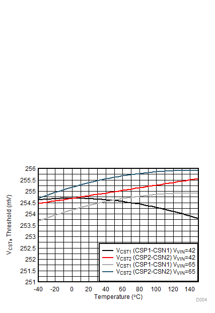
| VVIN = 42 V and 65 V | LEDx_PKTH_DAC = 255 | |
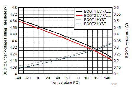
| VVIN = 42 V |
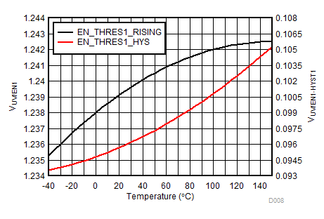
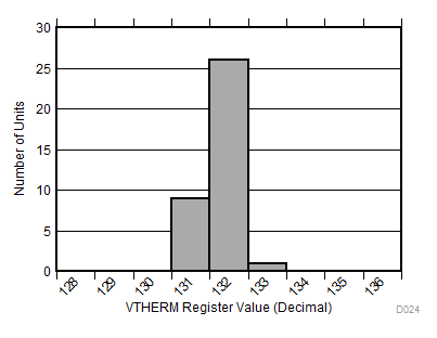
| TJ = 25°C |
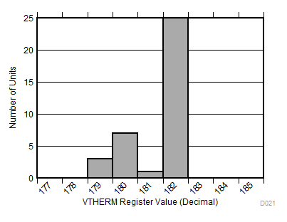
| TJ = 150°C |