SLUSCZ1 May 2017 TPS92518-Q1
PRODUCTION DATA.
- 1 Features
- 2 Applications
- 3 Description
- 4 Revision History
- 5 Pin Configuration and Functions
- 6 Specifications
- 7 Parameter Measurement Information
-
8 Detailed Description
- 8.1 Overview
- 8.2 Functional Block Diagram
- 8.3
Feature Description
- 8.3.1 General Operation
- 8.3.2 Important System Considerations: Off-Timer and Maximum Peak Threshold Values
- 8.3.3 Shunt FET or Matrix dimming: Maximum Off-timer Calculation
- 8.3.4 VIN and the VCC Internal Regulators
- 8.3.5 Output Enable Control Logic
- 8.3.6 BOOT Capacitor and BOOT UVLO
- 8.3.7 Drop-out Operation
- 8.3.8 Analog and PWM Dimming
- 8.3.9 VIN and CSPx Pin Configuration
- 8.3.10 Enable and Undervoltage Lock-out Configuration
- 8.3.11 Voltage Sampling and DAC Operation
- 8.3.12 Device Functional Modes
- 8.4 Serial Interface
- 8.5
Registers
- 8.5.1 CONTROL Register (Address = 00h) [reset = 00h]
- 8.5.2 STATUS (FAULT) Register (Address = 01h) [reset = 10h]
- 8.5.3 THERM_WARN_LMT Register (Address = 02h) [reset = 80h]
- 8.5.4 LED1_PKTH_DAC Register (Address = 03h) [reset = 80h]
- 8.5.5 LED2_PKTH_DAC Register (Address = 04h) [reset = 80h]
- 8.5.6 LED1_TOFF_DAC Register (Address = 05h) [reset = 80h]
- 8.5.7 LED2_TOFF_DAC Register (Address = 06h) [reset = 80h]
- 8.5.8 LED1_MAXOFF_DAC Register (Address = 07h) [reset = 80h]
- 8.5.9 LED2_MAXOFF_DAC Register (Address = 08h) [reset = 80h]
- 8.5.10 VTHERM Register (Address = 09h) [reset = 0h]
- 8.5.11 LED1_MOST_RECENT Register (Address = 0Ah) [reset = 0h]
- 8.5.12 LED1_LAST_ON Register (Address = 0Bh) [reset = 0h]
- 8.5.13 LED1_LAST_OFF Register (Address = 0Ch) [reset = 0h]
- 8.5.14 LED2_MOST_RECENT Register (Address = 0Dh) [reset = 0h]
- 8.5.15 LED2_LAST_ON Register (Address = 0Eh) [reset = 0h]
- 8.5.16 LED2_LAST_OFF Register (Address = 0Fh) [reset = 0h]
- 8.5.17 Reset Register (Address = 10h) [reset = 0h]
- 8.6 Programming
- 9 Application and Implementation
- 10Power Supply Recommendations
- 11Layout
- 12Device and Documentation Support
- 13Mechanical, Packaging, and Orderable Information
8 Detailed Description
8.1 Overview
The TPS92518-Q1 is a Dual Channel Buck LED controller with SPI Interface. Quasi-hysteretic operation allows a high control bandwidth and is ideal for Shunt FET and Matrix applications (series LED switched network). Internal DACs control the high-side differential peak current sense threshold, the peak-to-peak ripple (off-time) and the maximum off-time.
The high-side differential peak current sense threshold trip voltage is set via a 10:1 divider. The divider allows a lower sense voltage for improved efficiency while still allowing a practical control voltage. The device uses a controlled off-time (COFT) architecture to allow the converter to operate in both continuous conduction mode (CCM) and discontinuous conduction mode (DCM) with no external control loop compensation, and provides an inherent cycle-by-cycle current limit because of the peak current detection each cycle. Once an off-time (us·V) target is digitally programmed, analog circuitry adjusts the off-time to maintain a constant peak-to-peak ripple. Since the peak and ripple are fixed, regulation is maintained. The programmable off-time also controls the switching frequency target.
The digitally controlled analog peak current sense threshold allows analog dimming of the LED current over the full output range. The PWM dimming input allows for high-frequency PWM dimming control requiring no external components. An internal configurable maximum off-timer allows for easy implementation of external shunt FET dimming. Refer to shunt FET dimming information.This simple regulator contains all the features necessary to implement a high-efficiency, versatile, digitally controlled, high-performance LED driver.
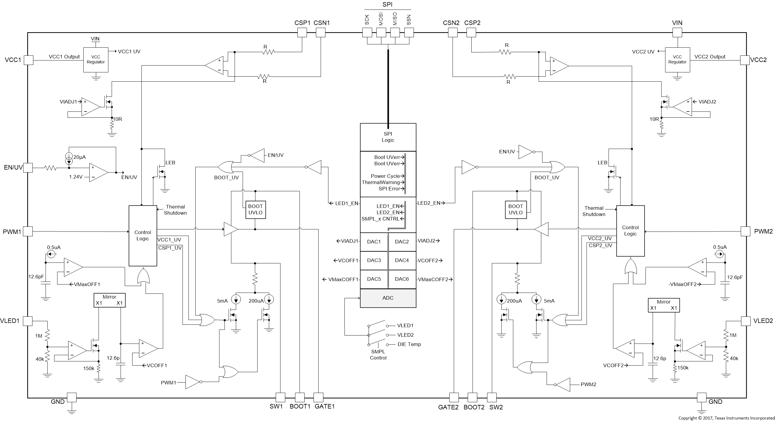
8.2 Functional Block Diagram
8.3 Feature Description
8.3.1 General Operation
The TPS92518-Q1 operates using a peak-current, constant off-time control as described in Figure 16. Two states dictate the high-side FET control. The switch turns on and stays on until the programmed peak current is reached. The peak current is controlled by monitoring the voltage across the sense resistor. When the voltage drop is higher than the programmed threshold, the peak current is reached. The switch is then turned OFF, which initiates an off-time period. An internal capacitor is then charged by a current source which varies in relation to the VLEDx pin voltage. When the capacitor voltage reaches the DAC controlled threshold, the off-time ends. The off-time capacitor resets and the main switch turns ON, starting the next ON cycle.
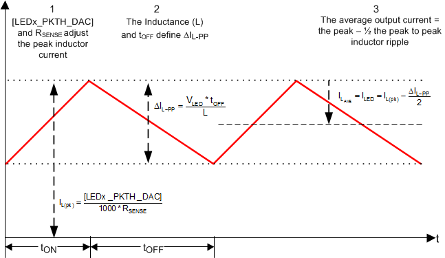 Figure 16. Hysteretic Operation
8.3.1.1 Constant Off-Time vs. Constant µs×V operation
Although commonly referred to as constant off-time, the off-time does vary with the output voltage in the standard TPS92518-Q1 configuration. This relation ensures constant peak-to-peak inductor current ripple (ΔIL-PP). Although not common, the VLEDx pin can be set to a fixed value to generate a truly constant off-time and limit changes in frequency, however current regulation degrades. To maintain regulation and a constant ripple over various output voltages, the converter off-time must become shorter or longer as VLEDx pin voltage changes. This results in a change in frequency. In this regard, the off-time register can be considered as a seconds-times-volts setting (s × V) for the converter. The TPS92518-Q1 Electrical Characteristics table specification for off-time specifies a certain off time duration for a certain register value. The time is also dependent on the VLEDx pin voltage. For example, the off-time is specified at 4 µs for a VVLEDx= 30 V and LEDx_TOFF_DAC = 255. The internal analog circuitry operates to keep the ripple and µs·V (micro-second volt) product constant. If the LEDx voltage changes to 15 V, the off time adjusts to 8 µs. If the LEDx voltage changes to 60 V the off time adjusts to 2 µs, and so on.
Two general cases can be examined: If the input voltage and output voltage are relatively constant, the frequency also remains constant. If either the input voltage or the output voltage changes, the frequency changes. For a fixed input voltage, the device operates at the maximum frequency at 50% duty cycle and the frequency reduces as the duty cycle becomes shorter or longer. A graphical representation is shown in Figure 17.
For a fixed output voltage (VVLEDx), the off-time stays fixed. The frequency then increases as the duty cycle becomes smaller with an increasing VIN voltage. This relation is shown in Figure 18.
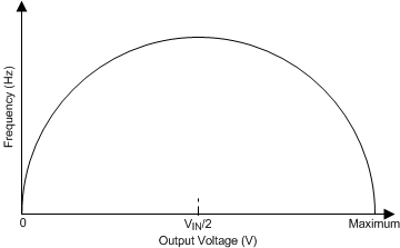 Figure 17. Frequency vs. LED Output Voltage. Fixed Input Voltage
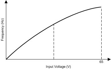 Figure 18. Frequency vs. Input Voltage. Fixed LED Voltage
8.3.1.2 Output Equation
By maintaining the off-time proportional to the output voltage (constant µs·V), it is possible to illustrate how the LED voltage (VLEDx) can be removed from the output current equation.
Starting with the inductor ripple derived from:

and the equation for the off-time:

the VLEDx term is then eliminated and the peak-to-peak inductor current ripple is defined by:

The final equation for the average LED current is then:

Because the control method relies on thresholds to control the main switch, offsets and delays must also be considered when examining the output accuracy. The ILED equation can be expanded to include these error sources as shown in Equation 5. ILED equations include several passive components, so it is important to consider the tolerance of each component. In this case the components are the main inductor and the sense resistor. The VCSTx-OFFSET parameter is the variation in the VCSTx threshold between the typical and maximum or minimum values as defined in the Electrical Characteristics. The peak current threshold delay (tDEL) and off timer trip point delay (tD-OFF) specifications are also shown in the Electrical Characteristics.

8.3.1.3 OFF Timer
The converter Off-time is controlled via the LEDx_TOFF_DAC[7:0] register and VLEDx pin. The VLEDx pin voltage is converted to a current that charges an internal capacitor to a voltage set by the LEDx_TOFF_DAC creating a delay. Details of this circuit are shown in the Functional Block Diagram. Deriving the off-time from the output voltage creates a ramp representing the inductor current.
When the TPS92518-Q1 is first enabled (All UVLO levels are cleared) both timer capacitor pull-downs are disabled allowing voltage to increase on the internal timer capacitors. When either capacitor reaches the matching DAC control voltage, the high-side FET is turned on, starting a switching cycle. The maximum off-time timer is always dominant at start-up when the output is completely discharged or when shunt FET dimming and the shunt FET shunts the output for the required period.
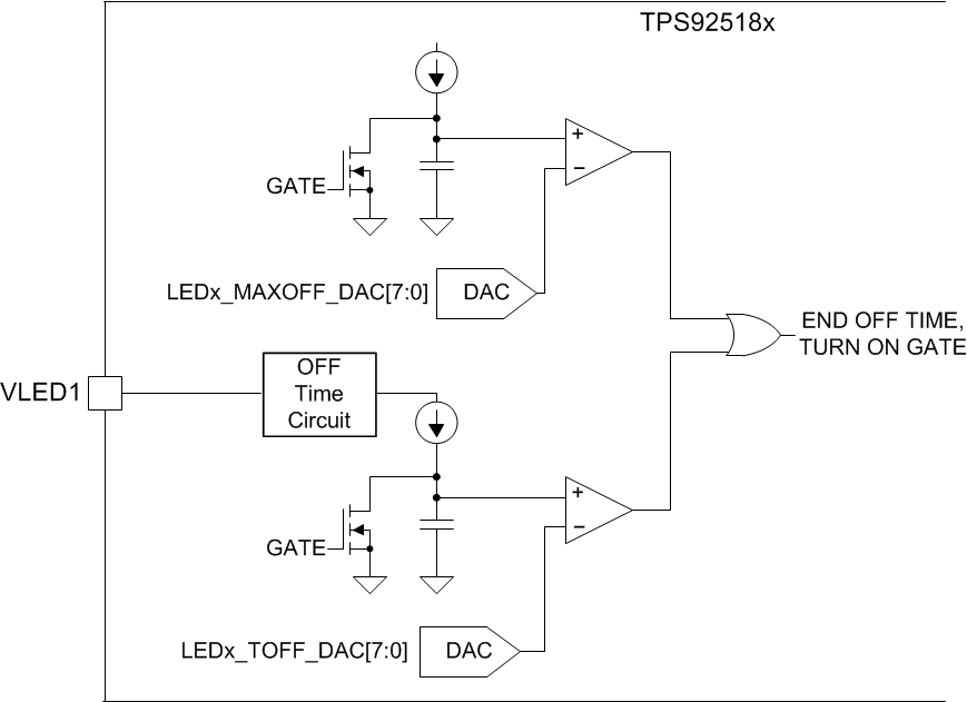 Figure 19. TPS92518-Q1 Simplified Internal Off-Timers Detail
8.3.1.3.1 Off-time and Maximum Off-time Calculations
Circuitry in the TPS92518-Q1 adjusts the off-time to ensure a constant peak-to-peak ripple. The off-time follows the relationship defined by Equation 6

Or

The maximum off-time circuit operates from its own independent current source that is not related to the VLEDx pin voltage. The equation for the maximum off-time is defined by Equation 8

8.3.2 Important System Considerations: Off-Timer and Maximum Peak Threshold Values
To allow full application flexibility, controls have not been implemented to limit values written to any SPI register. The system firmware must ensure control of all register values, but these two in particular must have safeguards in place.
Two potential application architectures that may allow a register modification after system engineering is complete are:
- A system has been engineered to allow firmware updates at a later time creating a situation where the Peak Current Threshold [LEDx_PKTH_DAC] value may be modified. The system LEDs can not support any higher than the designed current.
- A system has been engineered to allow fine tuning of the register values during a calibration step in manufacturing.
Section Peak Current Sense Comparator and Off-Time Thresholds - LEDx_TOFF_DAC and LEDx_MAXOFF_DAC discuss a few of many system approaches to ensure values remain correct.
8.3.2.1 Peak Current Sense Comparator
A comparator, two resistors and a current source create a peak current detection circuit block. See the Functional Block Diagram for details. A current source controlled by LEDx _PKTH_DAC[7:0] draws a current across a resistor in series with the comparator, forcing a proportional offset. The resistor in the current source (10 R) and in series with the comparator ( R ) are sized with a 10:1 ratio. This ratio allows for a practical voltage range of operation for the IADJ pin and maintains a small current sense voltage for low losses and less impact on efficiency. The ON cycle begins with the offset in place via IADJ across the resistor R at the VIN pin. When the current rises enough to create a voltage across the sense resistor to match the offset, the comparator trips. The end of the on-time period starts an off-time cycle.
Trace resistance can have an impact on accuracy, so care must be used when routing the traces to CSPx and CSNx from the sense resistor. Because the sense resistor value is typically in milli-ohms, use a short kelvin connection if possible.
8.3.2.2 Peak Current Threshold - LEDx _PKTH_DAC
- Always use a current sense resistor sized so the full scale current occurs at or close to the maximum value of 255. This is also a good practice for accuracy.
- Impose a limit in firmware. Monitor the LEDxPKTH_DAC variable before each write and ensure a maximum value is maintained.
8.3.2.3 Off-Time Thresholds - LEDx_TOFF_DAC and LEDx_MAXOFF_DAC
- Do not write '0' to the LEDx_TOFF_DAC or LEDx_MAXOFF_DAC registers. Writing a '0' to the LEDx_TOFF_DAC or LEDx_MAXOFF_DAC registers is the equivalent to: do not turn the FET off. Damage occurs to the device when a value of 0 is written to this register.
- Do not write an off-time value that causes the TPS92518-Q1 to operate beyond the maximum frequency possible for the conversion voltage ranges. For example: for a given application switching frequency and VIN to VLED conversion, there is a required duty cycle. If the duty cycle requirement is shorter than the TPS92518-Q1 minimum on-time ( tLEB ) current can not regulate. If the Off-time is made sufficiently short such that the inductor current is not able to reset given the V-s reached during the leading edge blanking time, the inductor current continues to increase until the inductor is saturated and the system may be damaged. The maximum frequency can be estimated, starting with Equation 9

Then the maximum frequency can be derived using the minimum on-time (tLEB leading edge blanking)

Using an example condition: VIN= 65 V, VLED= 6 V, tLEB= 250 ns, ΔIL-PP= 250 mA, we can find the maximum switching frequency and an Off-time minimum value.


The system controller must be programmed with a minimum LEDx_TOFF_DAC value of 55 allowing for some margin above the computed value of 53. (a smaller value = higher switching frequency) Note this is the correct value for this example. Each application is different. All register values, minimums and maximums must be considered for each application separately.
8.3.3 Shunt FET or Matrix dimming: Maximum Off-timer Calculation
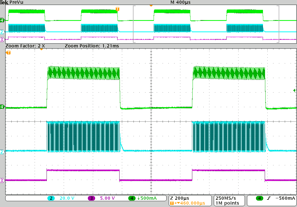
Shunt FET or Matrix dimming is typically used where precise control of the LED current is required. For the LED current and light output to most accurately match the control signal, the current source supplying the LEDs must be as close to ideal as possible. With the TPS92518-Q1 hysteretic control and maximum off-time setting, the LED current can approach ideal. Two waveforms show the result during shunt FET dimming with and without optimized maximum off-time control. The result with maximum off-time control is superior and approaches an ideal current source.
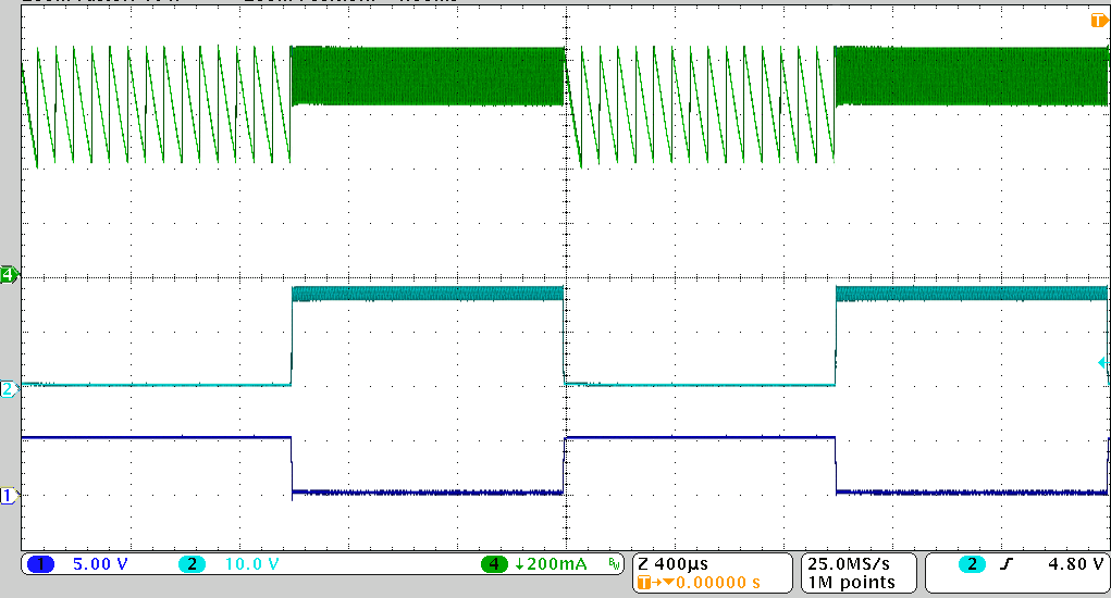
| CH4 (Green) : Inductor Current (200 mA per division) | CH2 (Cyan) : VVLEDx (10 V per division) | CH1 (Blue) : Shunt FET Control Signal |
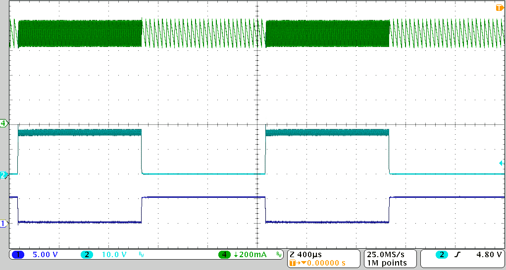
| CH4 (Green) : Inductor Current (200 mA per division) | CH2 (Cyan) : VVLEDx (10 V per division) | CH1 (Blue) : Shunt FET Control Signal |
To ensure the correct maximum off-time when shunt dimming it is necessary to calculate the off-time required when the output is in the shunted condition. The following procedure may be used:
- Estimate or measure the output voltage during the shunted condition.
- Compute the off-time required (tOFF-Shunt) when the output is shunted.
- Compute the Maximum Off-time Register Value.

Or for the Matrix approach:


8.3.3.1 Output Ringing and TPS92518-Q1 Protection
During shunt dimming, ringing may occur at the channel output due to PCB and device parasitic capacitances and inductances. This should be checked as part of the design process. If the ringing approaches the absolute maximum of any pin, a clamping diode must be added to the design. Connect the diode anode to the output at VLEDx and the cathode to the input voltage. This protection must also be used if the LED load is ever to be connected or removed while the output is enabled.
8.3.3.2 Live Peak and Off-Time Threshold Changes
All TPS92518-Q1 thresholds may be changed at any time. Once the SPI transaction completes, the change is seen in operation in ~100ns.
8.3.4 VIN and the VCC Internal Regulators
The device incorporates a linear regulator for each channel to generate the 7.5-V (typ) VCC voltage. Both VCC rails are powered from the VIN pin. VIN may be connected to the input of either channel or to a separate external supply. The VCC output voltages are internally monitored to implement undervoltage lockout (UVLO) protection for the respective channel. For example, if UVLO is reached on CH1, CH2 remains active. The VCC undervoltage lockout thresholds are fixed and cannot be adjusted.
The device has been designed to supply current for the device operation as well as additional power for external circuitry. If a 7.5-V rail is required in an application, the device can allow up to 500 μA to be drawn in addition to the device load. A capacitance of 1 μF or ≥ 10× the BOOT capacitance to a maximum of 10 μF is recommended.
The device requires adequate input decoupling in order to lower ΔVIN-PP ripple for the best VCC supply voltage performance. ΔVIN-PP must not exceed 10% of the input voltage or 3V, whichever is lower.
8.3.5 Output Enable Control Logic
Several safeguards and control states must be satisfied before switching can begin as shown in Figure 22. VCC, BOOT and the CSP input must not be in under voltage lock-out. The device must not be in thermal shut-down and the EN/UV pin must be high. The PWM pin for the channel must also be high. It is not possible to override the PWM pin logic via the SPI interface. If PWM dimming is not required, tie the pins to VCC.
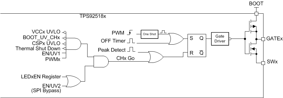 Figure 22. TPS92518-Q1 Output Enable Control
8.3.5.1 EN/UV2 - SPI Control Bypass
Note that the TPS92518-Q1 does allow a means to enable the part without SPI communication. By applying a voltage above the second threshold level, EN/UV2 (23.6 V typical), the state of the LEDxEN register is bypassed. This allows a TPS92518-Q1 to be powered and operated using the default register values (see Registers. A quick summary is that peak and off-time thresholds are set to 127 out of 255) without SPI communication. All other required operation points must still be satisfied as shown in Figure 22.
This could be useful in a manufacturing flow or during system troubleshooting. The logic path is highlighted again in Figure 23.
 Figure 23. Output Enable Control Logic
8.3.6 BOOT Capacitor and BOOT UVLO
The BOOT capacitor provides the power for the high-side gate drive circuitry. The capacitor is charged each cycle from VCC during the off-time phase of the switching cycle. During the off-time, the free-wheeling diode conducts, pulling the switchnode (SW) low and providing a conduction path to charge the capacitor. During the on-time, the current required to charge the high-side FET gate and power the driver are supplied by the capacitor.
A minimum boot capacitor can be calculated by considering: the MOSFET Qg, the driver quiescent current, and the desired nominal maximum on-time. Other factors include: the BOOT diode Vf, the minimum BOOT operation voltage, and the level of the switchnode (SWx) during the off-time. A rough estimate can be calculated using Equation 17: or just use 0.1µF.

The variables are defined by:
Table 1. CBOOT Variables
| Variable | Description |
|---|---|
| Qg | High-side FET total gate charge (Qg) as shown in the FET datasheet. |
| VCC | 7.5 V |
| VSW(off) | The switchnode voltage when the high-side FET is off. Use 0 V. |
| VBOOT-UVLO(MAX) | 5.2 V |
| IBOOT-Q | 200 µA |
| tON | Estimate your worst case on-time or use 500 µs |
| Vf(bd) | Forward drop of the boot diode |
A typical solution calculates a minimum CBOOT of approximately 60 nF, justifying the 100 nF selection.
If conditions are created which cause the boot capacitor to become depleted (see Drop-out Operation) and reach VBOOT-UVLO, switching is disabled until VBOOT increases by VBOOT-UVLO-HYST.
8.3.7 Drop-out Operation
If the input or output voltage change such that they become close to the same value, a condition known as drop-out is created. During drop-out conditions the output LED current may fall out of regulation. If the input reaches the target output voltage or below, the LED current can drop to zero. There are two stages of drop-out when operating with a hysteretic device like the TPS92518-Q1. The two stages are described in Early Drop-Out (Boot Capacitor Voltage >> VBOOT-UVLO) and Full Drop-Out (Boot Capacitor Voltage reaching VBOOT-UVLO).
8.3.7.1 Early Drop-Out (Boot Capacitor Voltage >> VBOOT-UVLO)
the first effects of drop-out can be seen when the input voltage approaches a few volts above the output voltage. Unless there is sufficient output capacitance, the change in the LED voltage during the ramp up of the inductor and output current can cause a non-linearity in the ramp.
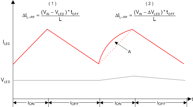 Figure 24. Inductor on-time Current Non-linearity
In case (1) shown in , VIN-VLED is sufficiently large that variations in VLED are not relevant and/or not present because of sufficient output capacitance.
In case (2), VIN and VLED are closer in value making the difference lower and more easily affected by variations in VLED. ΔVLED is the total variation in the voltage across the inductor and includes the ILED x RL-DCR voltage drop which also changes with IL and impacts the inductor current linearity. The combination of factors leads to an inductor current on-time non-linearity which increases the average value of the inductor current, and hence the LED current. This means the first affect of approaching drop-out is always an increase in LED current.
It is important to note that the output current is always limited to the peak limit set by the internal programmed reference and the sense resistor. (The peak current threshold) This means a design having a smaller overall inductor current ripple (smaller ΔIL-PP) will have less error when a drop-out condition occurs.
8.3.7.2 Full Drop-Out (Boot Capacitor Voltage reaching VBOOT-UVLO)
If VIN and VLED are sufficiently close the duty cycle demand increases. Because of the TPS92518-Q1 hysteretic control method, the high-side FET attempts to remain ON until the programmed peak current is reached. Keeping the high-side FET ON requires energy from the BOOT capacitor which depletes the BOOT capacitor voltage. If the high-side FET is ON for sufficient duration, the BOOT capacitor voltage eventually reaches VBOOT-UVLO level at which point the high-side FET is turned off. This allows for long on-times and duty cycles >99.5%, since the time the high-side FET can remain ON is long (>1 ms) compared to the time required the recharge the BOOT capacitor (approximately 100 ns). The typical maximum on-time can be estimated by Equation 18

8.3.7.3 Minimum BOOT Voltage and FET Control
The minimum VBOOT-UVLO is also the minimum voltage available to drive the external FET. Check the FET Output Characteristics (ID versus VDS) at the minimum BOOT voltage and ensure the FET is sufficiently enhanced under this condition. If the turn-on is marginal, the FET may operate in the linear region causing increased losses and possibly damage the device.
8.3.7.4 BOOT Controlled internal Pull-Down
Each time VBOOT ≤ VBOOT-UVLO an internal pull-down (IPD BOOTx = 5 mA typical) from the SWx pin to ground is enabled. This behavior occurs during drop-out conditions such as Full Drop-Out (Boot Capacitor Voltage reaching VBOOT-UVLO). This behavior also occurs at Start-Up if the output is pre-charged.
If the TPS92518-Q1 application uses an output capacitor and the output is disabled and re-enabled before the output voltage reduces (or is otherwise pre-charged) a condition can be created where the SWx pin voltage is not low enough for the BOOT capacitor to charge. (VSWx << VCC) BOOT-UV is then activated and the internal pull-down circuitry enabled. The pull-down circuitry reduces the time required to deplete the output voltage to allow the BOOT capacitor to be charged. Note that the internal pull-down circuitry can not act as a synchronous FET.
8.3.8 Analog and PWM Dimming
8.3.8.1 Dimming Methods
The TPS92518-Q1 has been designed to support three dimming methods. Analog, PWM and Shunt-FET or Matrix (TPS92661/TPS92662 device family) dimming. Analog dimming is still accomplished via the SPI interface through adjustment of the LEDx_PKTH_DAC register. PWM dimming is accomplished by using the PWMx pin. Shunt-FET or Matrix Dimming is optimized by using the LEDx_MAXOFF_DAC register. One or more dimming methods may also be combined to obtain extreme contrast ratios. To obtain an ultra-fine adjustment, the LEDxTOFF_DAC register may be also adjusted allowing average output current modifications in the range of 100 µA per LSB.
8.3.8.2 PWMx Pin Operation
PWM dimming can be used to adjust the output brightness by changing the applied PWM duty cycle to a channels’ corresponding PWM pin. Each channel can be controlled with an independent frequency and duty cycle.
When the PWM pin signal is < 0.8 V, the corresponding channel's gate logic is disabled. When PWM rises above 1.6 V the rising edge sets the gate drive latch and turns on the FET. If PWM dimming is not required, PWMx be tied to VCC.
Treat the PWM pin as a digital input. Avoid slow transitions of the pin voltage level around the logic thresholds. Ensure the signal edge rate is adequate (<100ns) when measured at the device PWMx pin to prevent false level interpretations. If the edge is too slow, a small capacitor may be required. If the PWM pin edge rate is too slow and is not adequately decoupled, the TPS92518-Q1 PWM pin logic may interpret one transition as multiple ON-OFF transitions. This can cause the output current to ratchet beyond the desired set-point and possibly cause the system to be damaged.
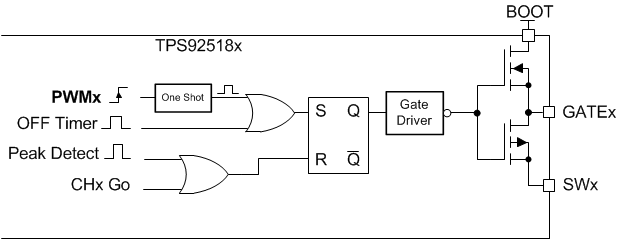 Figure 25. Gate Control Logic
8.3.8.3 PWM Dimming - Current Rise Performance
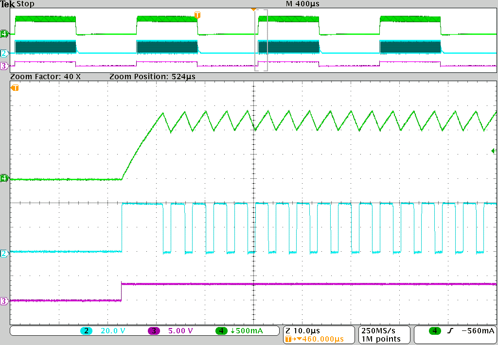
A unique feature of the TPS92518-Q1 hysteretic control allows the first switching pulse of a PWM dimming on-time to rise completely to the correct peak current in one switching cycle. An example is shown in Figure 26. When the rising edge of the PWM signal is seen by the PWMx pin the main FET is turned on. The FET remains ON until the programmed peak current threshold is reached. Once reached, switching continues until the PWMx pin voltage goes low. The TPS92518-Q1 can also operate when using pulse widths that are sufficiently narrow that the programmed peak is not reached. The on-time is terminated at the end of the PWM pulse and another on-time initiated when the PWMx pin goes high again.
8.3.8.4 PWM and Analog Dimming - Linearity Limitations and Buck Converters
8.3.8.4.1 PWM:
A linearity limitation occurs at very small PWM duty cycles; the PWM dimming on-time becomes short enough that it contains only one or a few switching cycles. If the PWMx pulse falls during an off-time (see Figure 28), the pulse length is not able to change because the switch is already off. This can lead to a small 'stair-case' dimming curve in this region as the duty cycle affects the average current during on-times and then not during off-times. This situation can be improved by increasing the switching frequency. This limitation is common to all Buck converters during very small PWM dimming duty cycles.
Shunt FET PWM dimming avoids this issue as the average current is affected during switching ON and OFF times. Shunt FET PWM dimming can out-perform PWM dimming, but is more complicated to implement.
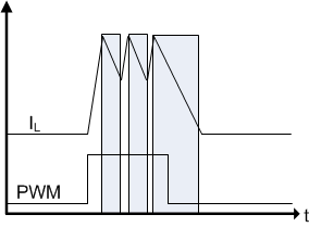 Figure 28. PWM Dimming Limitation
8.3.8.4.2 ANALOG:
Another impact on linearity can occur when analog dimming (LEDx_PKTH_DAC threshold adjustment) and the inductor current becomes discontinuous. Discontinuous conduction mode (DCM) occurs when the inductor current reaches 0 A each off-time. When the device enters DCM, the output current is no longer the peak current minus half the ripple current (as shown in Figure 16) and is no longer a linear relationship between the LEDx_PKTH_DAC value and the average output current. The linear range can be extended by lowering the ripple, ΔIL-PP to extend the natural linear region of operation.
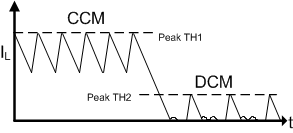 Figure 29. Analog Dimming Limitation
Another approach can be used by first analyzing the system operation. The point at which DCM is entered can be calculated as well as the average current value when in DCM. The micro-controller writing the LEDx_PKTH_DAC values can simply write alternate values in the DCM area to ensure net linear response to the LED average current. See DCM Current Calculation for information on calculating the average current when in DCM.
8.3.8.5 DCM Current Calculation
The converter is considered to be operating in DCM (Discontinuous conduction mode) when the peak current is less than the peak-to-peak inductor current ripple. (IL(pk) < ΔIL-PP). Equations Equation 20 through Equation 25 define the calculation described by Equation 19. Note that the value of the LED voltage is different when operating in DCM.
Starting with the basic equation for a buck converter in DCM:

followed by: (η is the estimated converter efficiency):


Where T defines the switching converter period.


See Equation 4 for the CCM (continuous current mode) equation.
8.3.8.6 Current Sharing
The TPS92518-Q1 can be configured to operate as a Two Channel, Single Output converter by configuring each channel identically and connecting the outputs together. Figure 30 illustrates the current sharing capability with each channel handling approximately the equal share of the output current load. Statistics are enabled and the average inductor current of each channel is also shown. The total output current for this configuration is 438 mA. Note that both channels must be enabled at the same time to allow charging of the boot capacitors. When a channel is paralleled, it may not be enabled after the first channel is enabled.
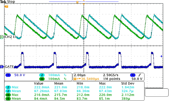
| CH4 (Green) : Inductor Current (100 mA per division) | CH1 (Blue) : SW1 Node (50 V per division) |
| CH2 (Cyan) : Inductor Current (100 mA per division) |
8.3.9 VIN and CSPx Pin Configuration
The TPS92518-Q1 has been designed to support single or dual input voltage sources. The VIN pin connection is also flexible and may be connected to the input supply of either channel or from a third independent channel.
The Electrical Characteristics table defines CSPUVLO as the minimum voltage required by a channel to continue operating. This limit is set regardless of the VIN and VCCx voltages. The VIN pin does not have an under voltage lock-out level, but must support the VCCx voltage for the channel. The minimum VIN pin voltage is limited to 6.5 V because two items depend on the voltage level for operation that have their own UVLO (under voltage lock-out) levels: VCCx and BOOTx. The 6.5-V level is derived from the maximum VCCx_UVLO level with some added margin. Alternately the maximum VBOOT-UVLO level may be used. If we consider this level and add the drop of the boot diode, we obtain the same value and with some margin obtain the same VIN pin minimum level of 6.5 V.
8.3.10 Enable and Undervoltage Lock-out Configuration
If drop-out operation is not desired, configure a resistor divider to disable switching of both channels at the desired input voltage.
The value of resistors R2 and R3 establish the undervoltage lockout level as shown in Figure 31. Include a small level of capacitance (approximately 0.1 μF) at the UVLO pin for noise immunity. If the application does not require drop-out operation (operation when VVIN approximates VVLEDx) program a UVLO level that allows no switching to occur until there is adequate input voltage available.
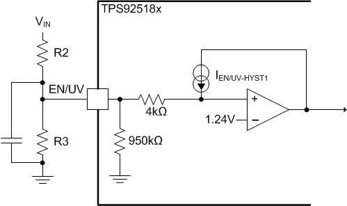 Figure 31. EN/UV Programming Resistors
Select the desired amount of voltage hysteresis and the desired turn-ON threshold (VIN-RISE_THRESHOLD). Because of the small amount of fixed-voltage hysteresis and fixed-hysteresis current, some combinations of turn-ON and turn-OFF thresholds are not possible. If the calculation results in values that are zero or negative, the combinations selected are not possible. After selecting a turn-ON point and desired amount of voltage hysteresis (VHYST) use Equation 26 and Equation 27 to calculate R3 and R2.


8.3.11 Voltage Sampling and DAC Operation
The TPS92518-Q1 integrates an ADC (analog to digital converter) and 6 DACs (digital to analog converters). The single ADC is multiplexed to provide the VLEDx pin voltages (starting with: LED1 Voltage) and the TPS92518-Q1 die temperature (Die Temperature Reading). A simplified diagram is shown in Figure 32.
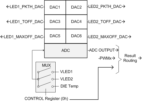 Figure 32. TPS92518-Q1 Internal Digital Blocks
8.3.11.1 ADC Control and LED Voltage Updating
Each of the analog outputs are controlled via their own individual DAC. The DAC's operate asynchronously and changes to controlling register values are updated immediately (~1 µs).
The ADC (analog to digital converter) sampling intervals are asynchronous to the incoming PWM1 and PWM2 signals. The TPS92518-Q1 logic determines which register(s) to update based on the state of the corresponding PWM signal at the time of ADC sampling. There are three LED voltage registers per channel:
- LEDx_MOST_RECENT
- LEDx_LAST_ON
- LEDx_LAST_OFF
The LEDx_LAST_ON registers are only updated when the corresponding PWM input has toggled from high to low, and the LEDx_LAST_OFF registers are only updated when the corresponding PWM input has toggled from low to high. This allows the last sample before the falling edge of PWM to be saved as the LAST_ON value, and the last sample before the rising edge of PWM to be saved as the LAST_OFF value ensuring the most consistent LED voltage reading.
8.3.12 Device Functional Modes
8.3.12.1 Analog Dimming
Analog dimming refers to the method of controlling the peak inductor current as the method to set the continuous average output current. Analog dimming is controlled digitally via the SPI interface. The register control value is converted via a digital to analog converter and the peak inductor current is compared to this analog voltage level. The level can be updated at any time during operation.
8.3.12.2 PWM Dimming
PWM Dimming is accomplished via a channel's corresponding PWM pin. A 1.6-V (typical) rising threshold and a 0.8-V (typical) falling threshold are required.
8.4 Serial Interface
The 4-wire control interface is compatible with the Serial Peripheral Interface (SPI) bus. The control bus consists of four signals: SSN, SCK, MOSI, and MISO. The SSN, SCK, and MOSI pins are TTL inputs into the TPS92518-Q1 while the MISO pin is an open-drain output. The SPI bus can be configured for both star-connect and daisy chain hardware connections.
A bus transaction is initiated by a MCU on a falling edge of SSN. While SSN is low, the input data present on the MOSI pin is sampled on the rising edge of SCK, MSbit first. The output data is asserted on the MISO pin at the falling edge of SCK. The figure below shows the data transition and sampling edges of SCK.
A valid transfer requires a non-zero integer multiple of 16 SCK cycles (i.e., 16, 32, 48, etc.). If SSN is pulsed low and no SCK pulses are issued before SSN rises, a SPI error is reported. Similarly, if SSN is raised before the 16th rising edge of SCK, the transfer is aborted and a SPI error is reported. If SSN is held low after the 16th falling edge of SCK and additional SCK edges occur, the data continues to flow through the TPS92518-Q1 shift register and out the MISO pin. When SSN transitions from low-to-high, the internal digital block decodes the most recent 16 bits that were received prior to the SSN rising edge.
SSN must transition high only after a multiple of 16 SCK cycles for a transaction to be valid and not set the SPI error bit. In the case of a write transaction, the TPS92518-Q1 logic performs the requested operation when SSN transitions high. In the case of a read transaction, the read data is transferred during the next frame, regardless of whether a SPI error has occurred.
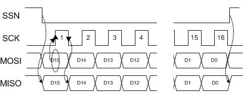 Figure 33. SPI Data Format
The data bit on MOSI is shifted into an internal 16-bit shift register (MSbit first) while data is simultaneously shifted out the MISO pin. While SSN is high (bus idle), MISO is tri-stated by the open-drain driver. While SSN is low, MISO is driven according to the 16-bit data pattern being shifted out based on the prior received command. At the falling edge of SSN to begin a new transaction, MISO is driven to the MSbit of the outbound data, and is updated on each subsequent falling edge of SCK.
NOTE
The first MISO transition happens on the first falling edge AFTER the first rising edge of SCK.
8.4.1 Command Frame
There is only one defined format for frames coming in on MOSI from the master. These are called Command frames. A Command frame can be either a read command or a write command.
A Command frame consists of a CMD bit, five bits of ADDRESS, a PARITY bit (odd parity), and nine bits of DATA. The format of the Command frame is shown in Figure 34. The bit sequence is as follows:
- The COMMAND bit (CMD). CMD = 1 means the transfer is a write command; CMD = 0 means it is a read command.
- The five-bit read or write ADDRESS (A4..A0).
- The PARITY bit (PAR). This bit is set by the following equation: PARITY = XNOR(CMD, A4..A0, D8..D0).
- Nine bits of read or write DATA (D8..D0). For a read, all data bits must be 0.
Both the Read Command and the Write Command follow the Command frame format as shown in Figure 34.
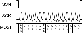 Figure 34. Command Frame Format
8.4.2 Response Frame Formats
There are three possible response frame formats: Read Response, Write Response and Write Error/POR. These formats are further described below.
8.4.2.1 Read Response Frame Format
The Read Response frame has the following format. The read response frame contains the state of the four fault bits. A special command is not required to poll the status of the bits, they are returned in every read response.
- The SPI Error bit (SPE).
- Two reserved bits (always 1).
- The POWER CYCLED bit PC).
- The LED2 BOOTUV ERROR bit (UV2).
- The LED1 BOOTUV ERROR bit “UV1).
- The THERMAL WARNING bit (TW).
- Nine bits of DATA (D8..D0).
This is shown in Figure 35 below. This frame is sent out by the TPS92518-Q1 following a read command.
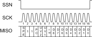 Figure 35. Read Response Frame Format
8.4.2.2 Write Response Frame Format
The Write Response frame has the following format:
- The SPI Error bit (SPE).
- The COMMAND bit (CMD).
- Five bits of ADDRESS (A4..A0).
- Nine bits of DATA (D8..D0).
This is shown in Figure 36. This frame is sent out following a write command if the previously received frame was a write command and no SPI Error occurred during that frame.
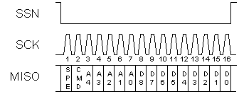 Figure 36. Write Response Frame Format
8.4.2.3 Write Error/POR Frame Format
The Write Error/POR frame is simply a ‘1’ in the MSB, followed by all zeroes (see Figure 37) This frame is sent out by the TPS92518-Q1 Internal digital block during the first SPI transfer following power-on reset, or following a write command with a SPI Error.
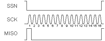 Figure 37. Write Error/POR
8.4.2.4 SPI Error
The TPS92518-Q1 records a SPI Error if any of the following conditions occur:
• The SPI command has a non-integer multiple of 16 SCK pulses.
• Any of the DATA bits during a read command are non-zero.
• There is a parity error in the previously received command.
If any of these conditions are true, the TPS92518-Q1 sets the SPI_ERROR bit in the Status Register. This is reported by setting the SPE (MSbit) in the next response frame. A write command with a SPI Error (not 16-bit aligned or bad parity) does NOT write to the register being addressed. The bad write is ignored and discarded. The TPS92518-Q1 attempts to respond to read requests regardless of SPI Error status since there is no danger to the system.
The SPI_ERROR bit can be cleared by reading the STATUS register.
8.5 Registers
Table 2 lists the memory-mapped registers. All register offset addresses not listed in Table 2 are considered as reserved locations and the register contents should not be modified.
Table 2. Registers
| Address | Acronym | Register Name | Section |
|---|---|---|---|
| 0h | CONTROL | Control Register | Go |
| 1h | STATUS | Status Register | Go |
| 2h | THERM_WARN_LMT | Thermal Warning Limit Register | Go |
| 3h | LED1_PKTH_DAC | LED1 Peak Threshold DAC Register | Go |
| 4h | LED2_PKTH_DAC | LED2 Peak Threshold DAC Register | Go |
| 5h | LED1_TOFF_DAC | LED1 Off Time DAC Register | Go |
| 6h | LED2_TOFF_DAC | LED2 Off Time DAC Register | Go |
| 7h | LED1_MAXOFF_DAC | LED1 Maximum Off Time DAC Register | Go |
| 8h | LED2_MAXOFF_DAC | LED2 Maximum Off Time DAC Register | Go |
| 9h | VTHERM | VTHERM Register | Go |
| Ah | LED1_MOST_RECENT | LED1 Most Recent Register | Go |
| Bh | LED1_LAST_ON | LED1 Last ADC On Register | Go |
| Ch | LED1_LAST_OFF | LED1 Last ADC Off Register | Go |
| Dh | LED2_MOST_RECENT | LED2 Most Recent ADC Register | Go |
| Eh | LED2_LAST_ON | LED2 Last On ADC Register | Go |
| Fh | LED2_LAST_OFF | LED2 Last Off ADC Register | Go |
| 10h | RESET | Reset Register | Go |
8.5.1 CONTROL Register (Address = 00h) [reset = 00h]
CONTROL is shown in Figure 38 and described in Table 3.
Return to Summary Table.
| 8 | 7 | 6 | 5 | 4 | 3 | 2 | 1 | 0 |
| RESERVED | THERM SMPL EN |
VLED2 SMPL EN |
VLED1 SMPL EN |
LED2 EN |
LED1 EN |
|||
| R-0h | R/W-0h | R/W-0h | R/W-0h | R/W-0h | R/W-0h | |||
Table 3. CONTROL Register Field Descriptions
| Bit | Field | Type | Reset | Description |
|---|---|---|---|---|
| 8-5 | RESERVED | R | 0 |
Reserved |
| 4 | THERM_SMPL_EN | R/W | 0 |
Thermal sample enable 0 = Disable sampling 1 = Enable sampling |
| 3 | VLED2_SMPL_EN | R/W | 0 |
VLED2 sample enable 0 = Disable sampling 1 = Enable sampling |
| 2 | VLED1_SMPL_EN | R/W | 0 |
VLED1 sample enable 0 = Disable sampling 1 = Enable sampling |
| 1 | LED2_EN | R/W | 0 |
LED2 enable. This bit controls the operation state of channel 2. 0 = Disable LED channel 2 1 = Enable LED channel 2 |
| 0 | LED1_EN | R/W | 0 |
LED1 enable. This bit controls the operation state of channel 1. 0 = Disable LED channel 1 1 = Enable LED channel 1 |
xSMPL_EN: The TPS92518-Q1 Analog to Digital Converter (ADC) input is multiplexed between 3 inputs: the thermal sensor and the two output voltages. Each input is sampled consecutively. Sampling a single input increases the sampling frequency. For example: an ADC sample and conversion requires ~100us. If one item is selected it is sampled at roughly 10 kHz. If all three inputs are selected each is sampled at ~3.3 kHz.
LEDx_EN: The TPS92518-Q1 PWMx pin AND the corresponding LEDxEN bit must be high for a channel to be enabled. If not using the external PWM input, tie the pin to VCC. The use of the LEDxEN register also enables the corresponding channel SWx pin internal pull-down to ensure no current flows to the LED load. A sample of the timing and waveforms around a SPI enable write are shown in Figure 39.
LEDxEN control may be bypassed using an analog activated override via the EN/UV pin. By applying a voltage >VEN/UV2 (23.6 V Typical) the contents of LEDxEN are ignored and the TPS92518-Q1 operates without SPI communication using the default register values. This is discussed in EN/UV2 - SPI Control Bypass
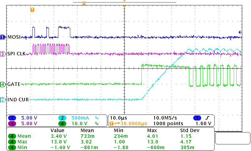 Figure 39. SPI Enable Write Waveform Example
8.5.2 STATUS (FAULT) Register (Address = 01h) [reset = 10h]
STATUS is shown in Figure 40 and described in Table 4.
Return to Summary Table.
| 8 | 7 | 6 | 5 | 4 | 3 | 2 | 1 | 0 |
| RESERVED | POWER CYCLED |
LED2BOOTUV ERROR |
LED1BOOTUV _ERROR |
THERMAL _ WARNING |
SPI _ERROR |
|||
| R-0h | RtoCl-1h | RtoCl-0h | RtoCl-0h | RtoCl-0h | RtoCl-0h | |||
Table 4. STATUS Register Field Descriptions
| Bit | Field | Type | Reset | Description |
|---|---|---|---|---|
| 8-5 | RESERVED | R | 0 |
Reserved |
| 4 | POWER_CYCLED | RtoCl | 1 |
Power cycled. This bit indicates that a power-on reset has occurred since the last STATUS register read. 0h = No power cycle has occurred since the last STATUS read. 1h = A power cycle has occurred since the last STATUS read. |
| 3 | LED2_BOOTUV_ERROR | RtoCl | 0 |
Latched LED2 BOOTUV error. This bit is cleared by reading the STATUS register if the condition is no longer present. |
| 2 | LED1_BOOTUV_ERROR | RtoCl | 0 |
Latched LED1 BOOTUV error. This bit is cleared by reading the STATUS register if the condition is no longer present. |
| 1 | THERMAL_WARNING | RtoCl | 0 |
Latched thermal warning flag: This bit is cleared by reading the STATUS register if the condition is no longer present. 0h = No thermal warning has occurred since the last STATUS read. 1h = A thermal warning has occurred since the last STATUS read. |
| 0 | SPI_ERROR | RtoCl | 0 |
Latched SPI error flag 0h = No SPI error occurred since the last STATUS read. 1h = A SPI error has occurred since the last STATUS read. |
POWER_CYCLED: This bit is set each time the input power is cycled to the TPS92518-Q1, including the first time the TPS92518-Q1 is powered on. To utilize this feature, read the bit as part of the start-up routine.
x_BOOTUV_ERROR: Set any time the high-side FET ‘BOOT’ drive circuit falls below VBOOT-UVLO (4.6 V typical). Note: This can be used to detect that the LED load is open, or that a drop-out condition is occurring. (any time VVIN ~= VVLEDx) For example: the LED load is removed from the output. There is no path for current flow and no increase of voltage on the sense resistor. The high-side FET remains ON requiring some current draw from the BOOT capacitor. After some time (milli-second magnitude) the capacitor is depleted, and reaches VBOOT-UVLO. At this point the high-side FET is turned off and the LEDx_BOOTUV_ERROR flag set. The boot capacitor is then be re-charged. See BOOT Capacitor and BOOT UVLO for more information.
SPI_ERROR: This error is cleared by reading the STATUS register. A SPI error is caused by any of the following conditions:
- A non-integer-multiple of 16 clocks received during a SPI transfer
- Any of the DATA bits are non-zero during a SPI read command
- SPI parity error during a SPI read or write command.
The TPS92518-Q1 detects and reports certain communication and system conditions. The SPI Error status is reported with every response frame. This is useful to quickly diagnose a communication problem and attempt to fix it. On a read response frame, the TPS92518-Q1 reports the Power Cycled, Boot UV and Thermal Warning status bits, as reflected in the STATUS register. Any power and/or system faults are immediately reported on ANY read response which allows the controlling MCU to more quickly respond to system problems. (See Read Response Frame Format)
8.5.3 THERM_WARN_LMT Register (Address = 02h) [reset = 80h]
THERM_WARN_LMT is shown in Figure 41 and described in Table 5.
Return to Summary Table.
| 8 | 7 | 6 | 5 | 4 | 3 | 2 | 1 | 0 |
| Reserved | THERM_WARN_LMT | |||||||
| R-0h | R/W-80h | |||||||
Table 5. THERM_WARN_LMT Register Field Descriptions
| Bit | Field | Type | Reset | Description |
|---|---|---|---|---|
| 8 | RSVD | R | 0 | Reserved |
| 7-0 | THERM_WARN_LMT | R/W | 80h |
Thermal warning voltage limit. If the ADC value of VTHERM ( Register 9h ) exceeds this limit, the THERMAL_ERROR bit in the STATUS register is set. |
THERM_WARN_LMT : The Thermal Warning status register is controlled by the content of this register.
Use Equation 28 to calculate the value for the register for the desired Thermal Warning Limit.

8.5.4 LED1_PKTH_DAC Register (Address = 03h) [reset = 80h]
LED1_PKTH_DAC is shown in Figure 42 and described in Table 6.
Return to Summary Table.
| 8 | 7 | 6 | 5 | 4 | 3 | 2 | 1 | 0 |
| Reserved | LED1_PKTH_DAC | |||||||
| R-0h | R/W-80h | |||||||
Table 6. LED1_PKTH_DAC Register Field Descriptions
| Bit | Field | Type | Reset | Description |
|---|---|---|---|---|
| 8 | RSVD | R | 0 | Reserved |
| 7-0 | LED1_PKTH_DAC | R/W | 80h |
Channel 1 peak threshold DAC value. |
The content of the register is used to set the peak inductor current (ILx-peak). The register value sets the voltage across the sense resistor (VCSPx-VCSNx) that ends the converter on-time.
The register value can be modified at any time during operation and the DAC analog value is then updated in ~1us. Always use the highest value that the application allows to reduce accuracy error. For example, the amount of variation in the actual peak threshold for LEDx_PKTH_DAC = 255 is less than for LEDx_PKTH_DAC = 127.
The Peak Current Threshold Voltage in volts (the voltage measured across the sense resistor that trips the peak current comparator) is simply the register value divided by 1000. (Consider the decimal register value to be in milli-volts)
The Peak Current Threshold in Amps can be calculated using Equation 29

8.5.5 LED2_PKTH_DAC Register (Address = 04h) [reset = 80h]
LED2_PKTH_DAC is shown in Figure 43 and described in Table 7.
Return to Summary Table.
| 8 | 7 | 6 | 5 | 4 | 3 | 2 | 1 | 0 |
| Reserved | LED2_PKTH_DAC | |||||||
| R-0h | R/W-80h | |||||||
Table 7. LED2_PKTH_DAC Register Field Descriptions
| Bit | Field | Type | Reset | Description |
|---|---|---|---|---|
| 8 | RSVD | R | 0 | Reserved |
| 7-0 | LED2_PKTH_DAC[7:0] | R/W | 80h |
Channel 2 peak threshold DAC value. |
The content of the register is used to set the peak inductor current (ILx-peak). The register value sets the voltage across the sense resistor (VCSPx-VCSNx) that ends the converter on-time.
The register value can be modified at any time during operation and the DAC analog value is then updated in ~1us. Always use the highest value that the application allows to reduce accuracy error. For example, the amount of variation in the actual peak threshold for LEDx_PKTH_DAC = 255 is less than for LEDx_PKTH_DAC = 10.
The Peak Current Threshold Voltage in volts (the voltage measured across the sense resistor that trips the peak current comparator) is simply the register value divided by 1000. (Consider the decimal register value to be in milli-volts)
The Peak Current Threshold in Amps can be calculated using Equation 30

8.5.6 LED1_TOFF_DAC Register (Address = 05h) [reset = 80h]
LED1_TOFF_DAC is shown in Figure 44 and described in Table 8.
Return to Summary Table.
| 8 | 7 | 6 | 5 | 4 | 3 | 2 | 1 | 0 |
| Reserved | LED1_TOFF_DAC | |||||||
| R-0h | R/W-80h | |||||||
Table 8. LED1_TOFF_DAC Register Field Descriptions
| Bit | Field | Type | Reset | Description |
|---|---|---|---|---|
| 8 | RSVD | R | 0 | Reserved |
| 7-0 | LED1_TOFF_DAC[7:0] | R/W | 80h |
Channel 1 off time DAC value. |
See LED2_TOFF_DAC Register (Address = 06h) [reset = 80h] for information on setting LED1_TOFF_DAC.
8.5.7 LED2_TOFF_DAC Register (Address = 06h) [reset = 80h]
LED2_TOFF_DAC is shown in Figure 45 and described in Table 9.
Return to Summary Table.
| 8 | 7 | 6 | 5 | 4 | 3 | 2 | 1 | 0 |
| Reserved | LED2_TOFF_DAC | |||||||
| R-0h | R/W-80h | |||||||
Table 9. LED2_TOFF_DAC Register Field Descriptions
| Bit | Field | Type | Reset | Description |
|---|---|---|---|---|
| 8 | RSVD | R | 0 | Reserved |
| 7-0 | LED2_TOFF_DAC[7:0] | R/W | 80h |
Channel 2 off time DAC value. |
LEDx_TOFF_DAC: The content of this register AND corresponding VLEDx pin set the corresponding channel off-time.
Important: →Ensure code controlling the TOFF register for both channels maintains limits on this register value. It is possible to write a value that is too low that may damage the application. See Off-Time Thresholds - LEDx_TOFF_DAC and LEDx_MAXOFF_DAC for more details about controlling this register value.

Where tOFF is in seconds. It can also be described as a setting for the channel V·µs product. The V·µs relation ensures the converter peak-peak ripple is constant and maintains the converter regulation.
8.5.8 LED1_MAXOFF_DAC Register (Address = 07h) [reset = 80h]
LED1_MAXOFF_DAC is shown in Figure 46 and described in Table 10.
Return to Summary Table.
| 8 | 7 | 6 | 5 | 4 | 3 | 2 | 1 | 0 |
| Reserved | LED1_MAXOFF_DAC | |||||||
| R-0h | R/W-80h | |||||||
Table 10. LED1_MAXOFF_DAC Register Field Descriptions
| Bit | Field | Type | Reset | Description |
|---|---|---|---|---|
| 8 | RSVD | R | 0 | Reserved |
| 7-0 | LED1_MAXOFF_DAC[7:0] | R/W | 80h |
Channel 1 maximum off time DAC value. |
See LED2_MAXOFF_DAC Register (Address = 08h) [reset = 80h] for information on setting the LED1_MAXOFF_DAC register.
8.5.9 LED2_MAXOFF_DAC Register (Address = 08h) [reset = 80h]
LED2_MAXOFF_DAC is shown in Figure 47 and described in Table 11.
Return to Summary Table.
| 8 | 7 | 6 | 5 | 4 | 3 | 2 | 1 | 0 |
| Reserved | LED2_MAXOFF_DAC | |||||||
| R-0h | R/W-80h | |||||||
Table 11. LED2_MAXOFF_DAC Register Field Descriptions
| Bit | Field | Type | Reset | Description |
|---|---|---|---|---|
| 8 | RSVD | R | 0 | Reserved |
| 7-0 | LED2_MAXOFF_DAC[7:0] | R/W | 80h |
Channel 2 maximum off time DAC value. |
LEDx_MAXOFF_DAC: the content of this register sets the maximum off-time for the corresponding channel, regardless of output voltage. LEDxMAXOFF and LEDx_TOFF operate in parallel. In normal operation, LEDxMAXOFF must always be longer in time than LEDxTOFF so as not to interfere with the normal operation of the converter.

The MaxOffTime value is most useful in LED Matrix or shunt-FET dimming applications. When the output LED voltage is sufficiently low (<2V), regular operation of the off-timer is not possible. This parallel timer does not rely on the output voltage and can be set to maintain consistent inductor current peak-to-peak ripple. Refer to the application section Off-Time Thresholds - LEDx_TOFF_DAC and LEDx_MAXOFF_DAC for equations to properly set the maximum off time under shunted conditions.
The Maximum off-time is also the time that must expire before the first cycle is initiated at start-up, or after a POR.
8.5.10 VTHERM Register (Address = 09h) [reset = 0h]
VTHERM is shown in Figure 48 and described in Table 12.
Return to Summary Table.
| 8 | 7 | 6 | 5 | 4 | 3 | 2 | 1 | 0 |
| Reserved | VTHERM | |||||||
| R-0h | R-0h | |||||||
Table 12. VTHERM Register Field Descriptions
| Bit | Field | Type | Reset | Description |
|---|---|---|---|---|
| 8 | RSVD | R | 0 | Reserved |
| 7-0 | VTHERM[7:0] | R | 0h |
Most recent ADC value of voltage on internal thermal sensor (based on a DeltaVBE). |
The content of the VTHERM register represents the TPS92518-Q1 die temperature. Use Equation 33 to convert to degrees Celsius. The conversion is approximately 2.5ºC per LSB. The part-to-part temperature reading variation is ±10ºC or ±4lsb. This is the maximum variation a population of parts will have at a given temperature. If a single part temperature is read and then the temperature changes and returns to the same temperature, the reading will vary ±1 lsb from the original reading.

8.5.11 LED1_MOST_RECENT Register (Address = 0Ah) [reset = 0h]
LED1_MOST_RECENT is shown in Figure 49 and described in Table 13.
Return to Summary Table.
| 8 | 7 | 6 | 5 | 4 | 3 | 2 | 1 | 0 |
| PWM1 | LED1_MOST_RECENT | |||||||
| R-0h | R-0h | |||||||
Table 13. LED1_MOST_RECENT Register Field Descriptions
| Bit | Field | Type | Reset | Description |
|---|---|---|---|---|
| 8 | PWM1 | R | 0 |
State of PWM1 when most recent ADC conversion of VLED1 voltage was started. |
| 7-0 | LED1_MOST_RECENT[7:0] | R | 0h |
Most recent ADC value of voltage on the VLED1 pin. |
This register contains the last LEDx reading recorded by the internal ADC along with the state of the corresponding PWM pin state at the time the value was recorded. See Voltage Sampling and DAC Operation for more detailed information about LED voltage sampling control. This sample occurs at anytime and is not co-ordinated with the PWMx input pin.

8.5.12 LED1_LAST_ON Register (Address = 0Bh) [reset = 0h]
LED1_LAST_ON is shown in Figure 50 and described in Table 14.
Return to Summary Table.
| 8 | 7 | 6 | 5 | 4 | 3 | 2 | 1 | 0 |
| Reserved | LED1_LAST_ON | |||||||
| R-0h | R-0h | |||||||
Table 14. LED1_LAST_ON Register Field Descriptions
| Bit | Field | Type | Reset | Description |
|---|---|---|---|---|
| 8 | RSVD | R | 0 | Reserved |
| 7-0 | LED1_LAST_ON[7:0] | R | 0h |
Last ADC value of voltage on VLED1 pin before falling edge of PWM1 |
Contains the last ADC recorded value of the LED1 voltage before the falling edge of PWM1. This ensures the most stable and consistent recorded value of the output voltage.

See Voltage Sampling and DAC Operation for more information on LED voltage sampling.
8.5.13 LED1_LAST_OFF Register (Address = 0Ch) [reset = 0h]
LED1_LAST_OFF is shown in Figure 51 and described in Table 15.
Return to Summary Table.
| 8 | 7 | 6 | 5 | 4 | 3 | 2 | 1 | 0 |
| Reserved | LED1_LAST_OFF | |||||||
| R-0h | R-0h | |||||||
Table 15. LED1_LAST_OFF Register Field Descriptions
| Bit | Field | Type | Reset | Description |
|---|---|---|---|---|
| 8 | RSVD | R | 0 | Reserved |
| 7-0 | LED1_LAST_OFF[7:0] | R | 0h | Last ADC value of voltage on VLED1 pin before rising edge of PWM1 |
Contains the last ADC recorded value of the LED1 voltage before the rising edge of PWM1. This ensures the most stable and consistent recorded value of the output voltage when the PWM signal was low.

See Voltage Sampling and DAC Operation for more information on LED voltage sampling.
8.5.14 LED2_MOST_RECENT Register (Address = 0Dh) [reset = 0h]
LED2_MOST_RECENT is shown in Figure 52 and described in Table 16.
Return to Summary Table.
| 8 | 7 | 6 | 5 | 4 | 3 | 2 | 1 | 0 |
| Reserved | LED2_MOST_RECENT | |||||||
| R-0h | R-0h | |||||||
Table 16. LED2_MOST_RECENT Register Field Descriptions
| Bit | Field | Type | Reset | Description |
|---|---|---|---|---|
| 8 | PWM2 | R | 0 |
State of PWM2 when most recent ADC conversion of VLED2 pin voltage was started. |
| 7-0 | LED2_MOST_RECENT[7:0] | R | 0h |
Most recent ADC value of voltage on the VLED2 pin. |
See section LED1_MOST_RECENT Register. Information on LED1_MOST_RECENT Register (Address = 0Ah) [reset = 0h] is the same as LED2_MOST_RECENT Register
8.5.15 LED2_LAST_ON Register (Address = 0Eh) [reset = 0h]
LED2_LAST_ON is shown in Figure 53 and described in Table 17.
Return to Summary Table.
| 8 | 7 | 6 | 5 | 4 | 3 | 2 | 1 | 0 |
| Reserved | LED2_LAST_ON | |||||||
| R-0h | R-80h | |||||||
Table 17. LED2_LAST_ON Register Field Descriptions
| Bit | Field | Type | Reset | Description |
|---|---|---|---|---|
| 8 | RSVD | R | 0 | Reserved |
| 7-0 | LED2_LAST_ON[7:0] | R | 0h |
Last ADC value of voltage on VLED2 pin before falling edge of PWM2 |
See section LED1_LAST_ON Register (Address = 0Bh) [reset = 0h] for more information on LED2_LAST_ON. Operation of each of the LAST_ONx registers is the same.
8.5.16 LED2_LAST_OFF Register (Address = 0Fh) [reset = 0h]
LED2_LAST_OFF is shown in Figure 54 and described in Table 18.
Return to Summary Table.
| 8 | 7 | 6 | 5 | 4 | 3 | 2 | 1 | 0 |
| Reserved | LED2_LAST_OFF | |||||||
| R-0h | R-0h | |||||||
Table 18. LED2_LAST_OFF Register Field Descriptions
| Bit | Field | Type | Reset | Description |
|---|---|---|---|---|
| 8 | RSVD | R | 0 | Reserved |
| 7-0 | LED2_LAST_OFF[7:0] | R | 0h |
Last ADC value of voltage on the VLED2 pin before rising edge of PWM2 |
See section LED1_LAST_OFF Register (Address = 0Ch) [reset = 0h] for more information on LED2_LAST_OFF. Operation of each of the LAST_OFFx registers is the same.
8.5.17 Reset Register (Address = 10h) [reset = 0h]
Reset is shown in Figure 55 and described in Table 19.
Return to Summary Table.
| 8 | 7 | 6 | 5 | 4 | 3 | 2 | 1 | 0 |
| Reset | ||||||||
| R/W-0h | ||||||||
Table 19. Reset Register Field Descriptions
| Bit | Field | Type | Reset | Description |
|---|---|---|---|---|
| 8 | Reset[8:0] | R/W | 0h |
Write 0x0C3 to the RESET register to reset all writable registers to their default values. This register is write-only. Reads of this register return 0. |
The RESET register provides a means to reset all the writable registers to their default values.
8.6 Programming
Coding examples outline common TPS92518-Q1 tasks.
8.6.1 TPS92518-Q1 Register Typedef - Sample Code
// TPS92518 Registers
typedef enum
{
			CONTROL = 0x00,
			STATUS = 0x01,
			THERM_WARN_LMT = 0x02,
			LED1_PKTH_DAC = 0x03,
			LED2_PKTH_DAC = 0x04,
			LED1_TOFF_DAC = 0x05,
			LED2_TOFF_DAC = 0x06,
			LED1_MAXOFF_DAC = 0x07,
			LED2_MAXOFF_DAC = 0x08,
			VTHERM = 0x09,
			LED1_MOST_RECENT = 0x0A,
			LED1_LAST_ON = 0x0B,
			LED1_LAST_OFF = 0x0C,
			LED2_MOST_RECENT = 0x0D,
			LED2_LAST_ON = 0x0E,
			LED2_LAST_OFF = 0x0F,
			RESET = 0x10
}Registers518;
8.6.2 Command Frame - Sample Code
The Command Frame can be constructed using the following code:
//assemble the 16-bit command
uint_t AssembleSPICmd(bool write, Registers518 regAddr, uint16_t data)
{
		uint16_t assembledCmd = 0; // Build this to shift through parity calc
		uint16_t parity = 0;       // Parity bit calculated here
		uint16_t packet = 0;       // This will be what we send

	// Set the CMD bit high if this is a write
	if(write)
	{
		assembledCmd |= 0x8000;  // Set CMD = 1
	}

	// Move the register address into the correct position
	assembledCmd |= (( regAddr << 10) & 0x7C00);

	// Append the data for a write
	if(write)
	{
		assembledCmd |= (data & 0x01FF);
	}

	// Save this off into the returned variable
	packet = assembledCmd;

	// Calculate the parity bit
	while(assembledCmd > 0)
	{
		// Count the number of 1s in the LSb
		if(assembledCmd & 0x0001)
		{
			parity++;
		}
		// Shift right
		assembledCmd >>= 1;
	}

	// If the LSb is a 0 (even # of 1s), we need to add the odd parity bit
	if(!(parity & 0x0001))
	{
		packet |= (1 << 9);
	}

	return(packet);
}
8.6.3 SPI Read/Write - Sample Code
Perform a SPI read/write; with assumption that the buffer holding write data has been filled using the AssembleSPICmd function, Then send the 16-bit characters. Lower numbered array elements are nearer the MCU in the daisy-chain.
/* Perform the SPI read/write; assumed that the buffer holding write data has been filled
 * using the AssembleSPICmd function. */

void SendSPIPacket(uint16_t chainID, uint16_t *writeBuf_ptr, uint16_t *readBuf_ptr)
{
		uint16_t i;

		// Which SSN to take low; SSx_LOW is a macro for GPO manipulation switch(chainID)
		{
		case 0:
			SS0_LOW();
			break;
		case 1:
			SS1_LOW();
			break;
		case 2:
			SS2_LOW();
			break;
		default:
			break;
		}

  // Send the 16-bit characters; lower numbered array elements are nearer the MCU in the daisy-chain
	for(i = NUM_DEVICES_PER_CHAIN; i >= 1; i--)
	{
		SpibRegs.SPITXBUF = *(writeBuf_ptr + (i-1));   // Send each 16-bit piece of the packet
		while(SpibRegs.SPISTS.bit.INT_FLAG == 0);      // Wait for buffer to empty
		*(readBuf_ptr + (i-1)) = SpibRegs.SPIRXBUF;    // Grab the TPS92518 response
	}

	// Small delay to ensure all data is shifted out
	DELAY_US(5);

	// Make sure all SSN#s are high (SSx_HIGH is a macro)
	SS0_HIGH();
	SS1_HIGH();
	SS2_HIGH();
}
