SLUSCZ1 May 2017 TPS92518-Q1
PRODUCTION DATA.
- 1 Features
- 2 Applications
- 3 Description
- 4 Revision History
- 5 Pin Configuration and Functions
- 6 Specifications
- 7 Parameter Measurement Information
-
8 Detailed Description
- 8.1 Overview
- 8.2 Functional Block Diagram
- 8.3
Feature Description
- 8.3.1 General Operation
- 8.3.2 Important System Considerations: Off-Timer and Maximum Peak Threshold Values
- 8.3.3 Shunt FET or Matrix dimming: Maximum Off-timer Calculation
- 8.3.4 VIN and the VCC Internal Regulators
- 8.3.5 Output Enable Control Logic
- 8.3.6 BOOT Capacitor and BOOT UVLO
- 8.3.7 Drop-out Operation
- 8.3.8 Analog and PWM Dimming
- 8.3.9 VIN and CSPx Pin Configuration
- 8.3.10 Enable and Undervoltage Lock-out Configuration
- 8.3.11 Voltage Sampling and DAC Operation
- 8.3.12 Device Functional Modes
- 8.4 Serial Interface
- 8.5
Registers
- 8.5.1 CONTROL Register (Address = 00h) [reset = 00h]
- 8.5.2 STATUS (FAULT) Register (Address = 01h) [reset = 10h]
- 8.5.3 THERM_WARN_LMT Register (Address = 02h) [reset = 80h]
- 8.5.4 LED1_PKTH_DAC Register (Address = 03h) [reset = 80h]
- 8.5.5 LED2_PKTH_DAC Register (Address = 04h) [reset = 80h]
- 8.5.6 LED1_TOFF_DAC Register (Address = 05h) [reset = 80h]
- 8.5.7 LED2_TOFF_DAC Register (Address = 06h) [reset = 80h]
- 8.5.8 LED1_MAXOFF_DAC Register (Address = 07h) [reset = 80h]
- 8.5.9 LED2_MAXOFF_DAC Register (Address = 08h) [reset = 80h]
- 8.5.10 VTHERM Register (Address = 09h) [reset = 0h]
- 8.5.11 LED1_MOST_RECENT Register (Address = 0Ah) [reset = 0h]
- 8.5.12 LED1_LAST_ON Register (Address = 0Bh) [reset = 0h]
- 8.5.13 LED1_LAST_OFF Register (Address = 0Ch) [reset = 0h]
- 8.5.14 LED2_MOST_RECENT Register (Address = 0Dh) [reset = 0h]
- 8.5.15 LED2_LAST_ON Register (Address = 0Eh) [reset = 0h]
- 8.5.16 LED2_LAST_OFF Register (Address = 0Fh) [reset = 0h]
- 8.5.17 Reset Register (Address = 10h) [reset = 0h]
- 8.6 Programming
- 9 Application and Implementation
- 10Power Supply Recommendations
- 11Layout
- 12Device and Documentation Support
- 13Mechanical, Packaging, and Orderable Information
9 Application and Implementation
NOTE
Information in the following applications sections is not part of the TI component specification, and TI does not warrant its accuracy or completeness. TI’s customers are responsible for determining suitability of components for their purposes. Customers should validate and test their design implementation to confirm system functionality.
9.1 Application Information
The TPS92518-Q1 buck current controller is suitable for implementing step-down LED drivers. This section presents a simplified design process for an LED driver with the specifications shown in Design Requirements:
Use the following design procedure to select component values for this and similar buck applications.
9.2 Typical Application
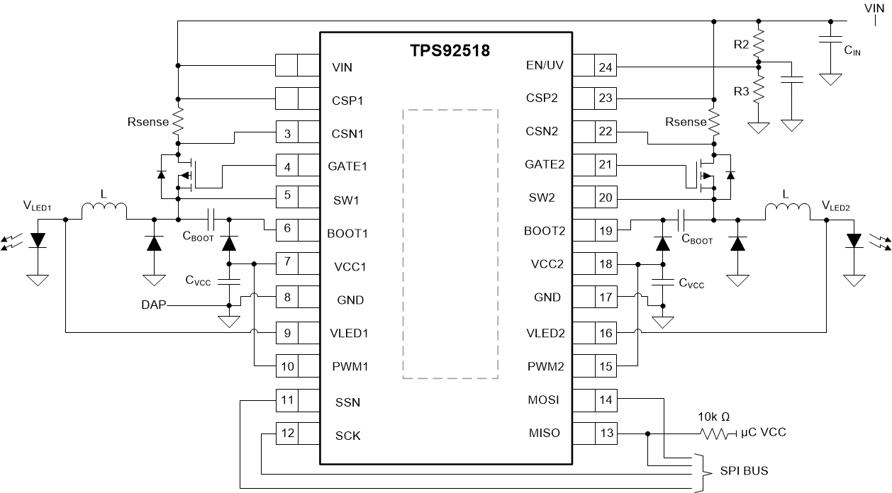
 Figure 56. Typical Application Schematic
9.2.1 Design Requirements
Buck converter topology.
Table 20. Design Requirements
| PARAMETER | VALUE | UNIT | |
|---|---|---|---|
| VIN | Input voltage | 50 | V |
| ILED | LED current | 1.6 | A |
| VLED | LED voltage | 9.4 | V |
| ΔIL-PP | Ripple voltage change | 12.5% | |
| LEDx_PK_DAC[7:0] | Target switching frequency | 550 | kHz |
| VEN/UV | 40 | V | |
| VEN/UV-HYST | 5 | V | |
9.2.2 Detailed Design Procedure
TPS92518-Q1 Design Equations and sample Calculations.
Start by calculating the converter Duty Cycle
-
Calculate D:
Equation 37.

-
Calculate Off Time Estimate:
- Using Switching Period (T)
- T = tOFF + tON = tOFF + (D x T), and T = 1/fSW
then:
Equation 38.
- Using Switching Period (T)
- Compute the off-time register value:
- Calculate the inductance: Where ΔIL-PP is in Amps.
- Calculate the sense resistor:For the highest current set-point, set the peak threshold register to be as high as possible. Use [LEDx_PKTH_DAC] = 255 (the maximum value) if possible to increase the converter accuracy. Only use something lower if it is possible the average current level requires adjustment after the design is complete and the BOM is complete. For example, if the production flow includes a trimming step.
- Calculate the UVLO Resistors: Considering the turn-on point of 40 V and a 5 V hysteresis values for the UVLO resistors can be selected. ( Refer to Figure 31 for configuration details.)


The user has the option of choosing a value of 68µH, however, this design uses the next common value of 100 µH in order to meet the ripple requirements. When selecting an inductor, ensure both the average and peak current values are met with adequate margin.


9.2.3 Application Curves

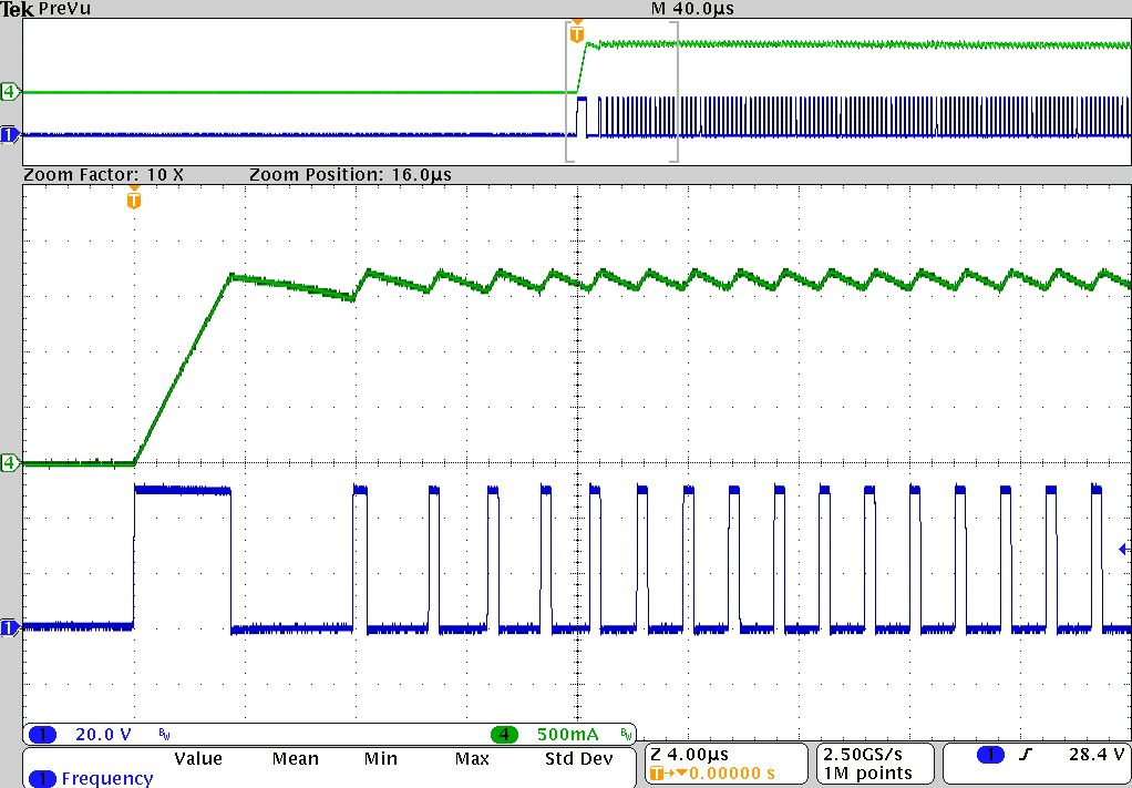
| CH4 (Green) : Inductor Current (500 mA per division) | CH1 (Blue) : SWx Node (20 V per division) | Time Base: 4µs per division |

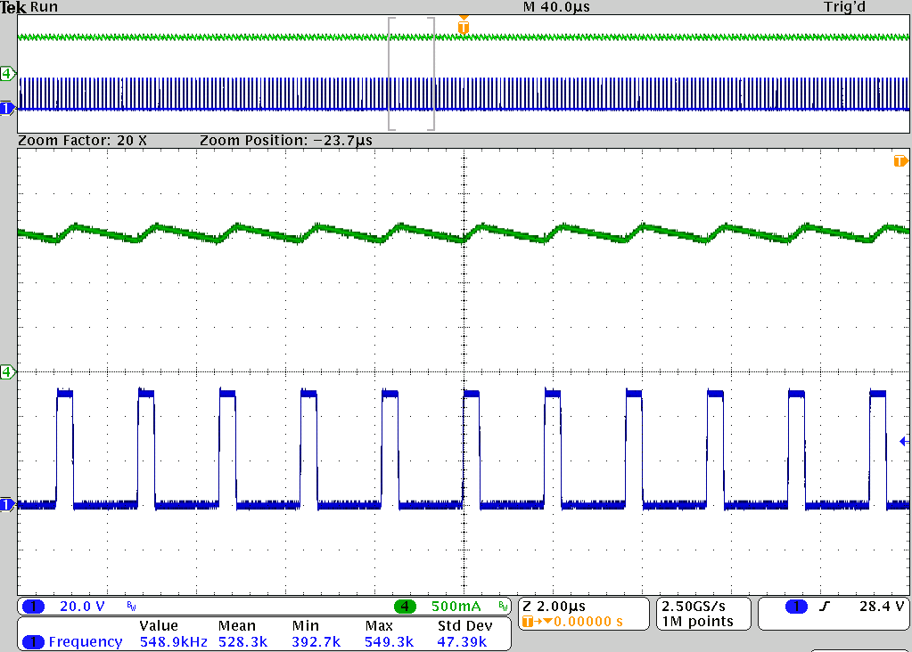
| CH4 (Green) : Inductor Current (500 mA per division) | CH1 (Blue) : SWx Node (20 V per division) | Time Base: 2µs per division |
TPS92518-Q1 Useful Equations:
Converter Output Equation (A) (Ideal)

Converter Output Equation (A) (With error sources)

9.3 Dos and Don'ts
Do:
- Check the TPS92518-Q1 case and junction temperature during and after prototyping of any solution.
- Check the soldering of the device thermal pad (DAP) in production
Don't:
- Don't write 0 (zero) to any of the off-time registers ([LEDx_TOFF_DAC] or LEDxMAXOFF_DAC] unless the use case is well understood and tested.