ZHCSFD3A April 2016 – August 2016 TPS92515 , TPS92515-Q1 , TPS92515HV , TPS92515HV-Q1
PRODUCTION DATA.
- 1 特性
- 2 应用
- 3 说明
- 4 修订历史记录
- 5 Device Comparison Table
- 6 Pin Configuration and Functions
- 7 Specifications
-
8 Detailed Description
- 8.1 Overview
- 8.2 Functional Block Diagram
- 8.3
Feature Description
- 8.3.1 General Operation
- 8.3.2 Current Sense Comparator
- 8.3.3 OFF Timer
- 8.3.4 OFF-Timer, Shunt FET Dimming or Shunted Output Condition
- 8.3.5 Internal N-channel MOSFET
- 8.3.6 VCC Internal Regulator and Undervoltage Lockout (UVLO)
- 8.3.7 Analog Adjust Input
- 8.3.8 Thermal Protection
- 8.3.9 Junction Temperature Relative Estimation
- 8.3.10 BOOT and BOOT UVLO
- 8.3.11 PWM (UVLO and Enable)
- 8.4 Device Functional Modes
-
9 Application and Implementation
- 9.1 Application Information
- 9.2
Typical Application
- 9.2.1 General Design Procedure
- 9.2.2 Design Requirements
- 9.2.3
Detailed Design Procedure
- 9.2.3.1 Calculating Duty Cycle
- 9.2.3.2 Calculate OFF-Time Estimate
- 9.2.3.3 Calculate OFF-Time Resistor ROFF
- 9.2.3.4 Calculate the Inductance Value
- 9.2.3.5 Calculate the Sense Resistance
- 9.2.3.6 Calculate Input Capacitance
- 9.2.3.7 Verify Peak Current for Inductor Selection
- 9.2.3.8 Calculate Output Capacitance
- 9.2.3.9 Calculate UVLO Resistance Values
- 9.2.4 Application Curves
- 9.3 Dos and Don'ts
- 10Power Supply Recommendations
- 11Layout
- 12器件和文档支持
- 13机械、封装和可订购信息
7 Specifications
7.1 Absolute Maximum Ratings
over operating free-air temperature range (unless otherwise noted)(1)| MIN | MAX | UNIT | ||
|---|---|---|---|---|
| VIN, DRN, SW, CSN to GND | TPS92515, TPS92515-Q1 | –0.3 | 45.0 | V |
| TPS92515HV, TPS92515HV-Q1 | –0.3 | 65.0 | ||
| DRN to SW | TPS92515, TPS92515-Q1 | –0.3 | 45.0 | |
| TPS92515HV, TPS92515HV-Q1 | –0.3 | 65.0 | ||
| BOOT to GND | TPS92515, TPS92515-Q1 | –0.3 | 50.5 | |
| TPS92515HV, TPS92515HV-Q1 | –0.3 | 70.5 | ||
| COFF, IADJ, PWM to GND | –0.3 | 5.5 | ||
| BOOT to SW | –0.3 | 5.5 | ||
| VCC to GND | -0.3 | 5.5 | ||
| VIN to CSN | –0.3 | 0.3 | ||
| SW to GND, 10-ns transient (2) | –2.0 | |||
| Storage temperature, Tstg | -40 | 150 | °C | |
(1) Stresses beyond those listed under Absolute Maximum Ratings may cause permanent damage to the device. These are stress ratings only, which do not imply functional operation of the device at these or any other conditions beyond those indicated under Recommended Operating Conditions. Exposure to absolute-maximum-rated conditions for extended periods may affect device reliability.
(2) DRN to SW. Absolute maximum not to be exceeded.
7.2 ESD Ratings
| VALUE | UNIT | |||
|---|---|---|---|---|
| V(ESD) | Electrostatic discharge | Human-body model (HBM), per AEC Q100-002(1) | ±2000 | V |
| Charged-device model (CDM), per AEC Q100-011 | ±750 | |||
(1) AEC Q100-002 indicates that HBM stressing shall be in accordance with the ANSI/ESDA/JEDEC JS-001 specification.
7.3 Recommended Operating Conditions
over operating free-air temperature range (unless otherwise noted)| MIN | NOM | MAX | UNIT | |||
|---|---|---|---|---|---|---|
| VIN | Input voltage | TPS92515, TPS92515-Q1 | 5.5 | 42 | V | |
| TPS92515HV, TPS92515HV-Q1 | 5.5 | 65 | ||||
| TA | Operating ambient temperature | 125 | °C | |||
| TJ | Operating junction temperature | 150 | °C | |||
7.4
Thermal Information
| THERMAL METRIC(1) | TPS92515 | UNIT | |
|---|---|---|---|
| HVSSOP | |||
| 10 PINS | |||
| RθJA | Junction-to-ambient thermal resistance | 56.2 | °C/W |
| RθJC(top) | Junction-to-case (top) thermal resistance | 44.7 | °C/W |
| RθJB | Junction-to-board thermal resistance | 32.1 | °C/W |
| ψJT | Junction-to-top characterization parameter | 1.5 | °C/W |
| ψJB | Junction-to-board characterization parameter | 31.8 | °C/W |
| RθJC(bot) | Junction-to-case (bottom) thermal resistance | 5.3 | °C/W |
(1) For more information about traditional and new thermal metrics, see the Semiconductor and device Package Thermal Metrics application report, SPRA953.
7.5 Electrical Characteristics
VIN = 40 V, –40°C ≤ TJ ≤ 150°C, VBOOT is referenced to SW pin, unless otherwise specified.| PARAMETER | TEST CONDITION | MIN | TYP | MAX | UNIT | |
| PEAK CURRENT COMPARATOR | ||||||
| VCST | VIN– VCSN peak current threshold | VIADJ = VCC | 224 | 240 | 251 | mV |
| VIADJ = 2.2 V | 211.5 | 220 | 223.5 | mV | ||
| AADJ | VIADJ to VIN – VCSN threshold gain | 0.1 ≤ VIADJ ≤ 2.2 V | 0.1 | V/V | ||
| ICSN | Current sense pin, input bias current | –5 | 0 | µA | ||
| tDEL | CSN pin falling delay | CSN fall to SW fall | 75 | 130 | ns | |
| tLEB | Minimum ON-time | Minimum pulse width | 75 | 195 | 275 | ns |
| SYSTEM CURRENTS | ||||||
| Icq | Operating current | Not switching, VIADJ = VVCC | 0.85 | 1.5 | mA | |
| INTEGRATED N-Channel MOSFET AND DRIVER | ||||||
| RDS(on) | FET ON-resistance | IDRN-SW = 200mA, VBOOT = 5 V, TJ = 25°C |
290 | 500 | mΩ | |
| IDRN-SW = 200mA, VBOOT = 5 V, TJ = 150°C |
290 | 600 | ||||
| IDRN-SW = 200mA, VBOOT = 3.5 V, TJ = 25°C |
310 | 500 | ||||
| IDRN-SW = 200mA, VBOOT = 3.5 V, TJ = 150°C |
310 | 650 | ||||
| IDRN-SW(off) | FET leakage current | VDRN-SW = 6 V, VSW = 0 V | 10 | µA | ||
| VBOOT-UVLO | Voltage where gate drive is disabled | VBOOT falling | 2.0 | 2.8 | 3.5 | V |
| VBOOT-UVLO(hys) | BOOT pin UVLO Hysteresis | 125 | mV | |||
| IPD(PWM/UVLO) | Pull down from SW when PWM low. | PWM low, VBOOT = 5 V , VSW = 8 V | 100 | 130 | µA | |
| IPD(BOOT) | Pull down from SW when VBOOT reaches VBOOT-UVLO | PWM high, VBOOT < BOOT-UVLO, VSW = 8 V | 5 | 7 | mA | |
| IBOOT_Q | BOOT pin quiescent current | VBOOT = 5.5 V, 0 V ≤ VSW ≤ 65 V | 60 | 90 | µA | |
| VCC/REFERENCE REGULATOR | ||||||
| VCC | Regulated pin voltage | IVCC(ext) ≤ 500 µA | 4.8 | 5.0 | 5.2 | V |
| VCCDO | Drop out voltage | IVCC(ext) ≤ 500 µA | 0.1 | 0.2 | V | |
| VCCUVLO | VCC undervoltage lockout | Falling threshold, VIN = 10 V | 4.0 | 4.2 | 4.4 | V |
| VCCUVLO_hys | VCC undervoltage lockout hysteresis | 0.22 | V | |||
| IVCC(ILIM) | VCC regulator current limit | VCC shorted to GND | 14 | 19 | 23 | mA |
| VINUVLO | VIN UVLO Falling Threshold | 4.65 | 4.90 | 5.15 | V | |
| VINUVLO_hys | VIN UVLO Hysteresis | 150 | 190 | 225 | mV | |
| OFF-TIMER | ||||||
| VOFT | OFF-time threshold | 0.95 | 1.00 | 1.05 | V | |
| tD(off) | COFF threshold | COFF to SW rising delay | 68 | 120 | ns | |
| tOFF(max) | Maximum OFF-time | 230 | µs | |||
| PWM/UVLO (Enable) | ||||||
| IPWM(uvlo) | PWM/UVLO pin current | VPWM(uvlo) = 5.5 V | 10 | nA | ||
| VPWM(uvlo) | PWM/UVLO pin threshold | PWM pin rising | 0.95 | 1.0 | 1.05 | V |
| VPWM(uvlo-hys) | PWM/UVLO pin hysteresis | Difference between rising and falling threshold | 50 | 100 | 150 | mV |
| tPWM(uvlo) | PWM/UVLO pin delay | PWM pin rising to SW pin rising | 75 | 130 | ns | |
| PWM pin falling to SW pin falling | 100 | 170 | ns | |||
| IPWM(uvlo-hys) | PWM/UVLO hysteresis current | VPWM(uvlo) = 2 V | –25 | –20 | –15 | μA |
| THERMAL SHUTDOWN | ||||||
| TSD | Thermal shutdown temperature | 175 | °C | |||
| TSD(hyst) | Thermal shutdown hysteresis | 10 | ||||
7.6 Typical Characteristics
TJ = TA = 25°C unless otherwise specified. Characteristics are identical for TPS92515x and TPS92515HVx. VIN >42 V curves apply to TPS92515HVx only.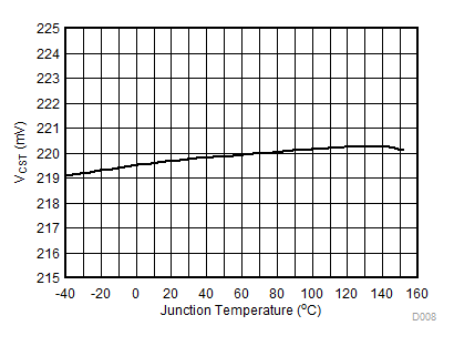
| VIADJ = 2.2 V | VIN = 40 V |
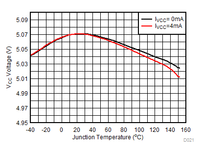
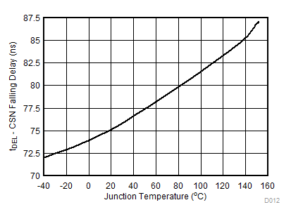
| VIN = 6 V |
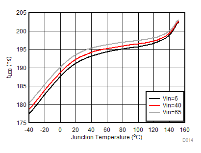
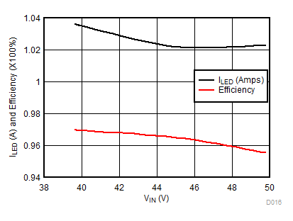
| VLED = 35 V | VIADJ=2.4 V | RSENSE = 0.196 Ω |
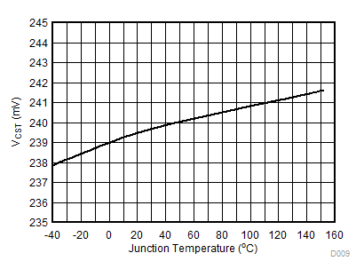
| VIADJ = VCC | VIN = 40 V |
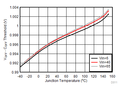
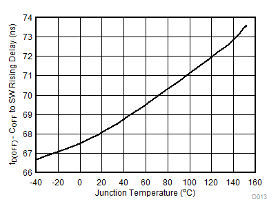
| VIN = 40 V |
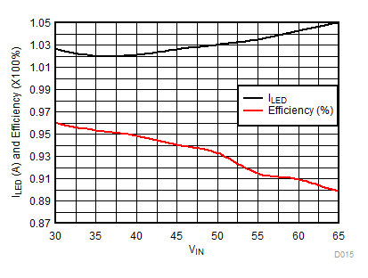
| VLED = 22 V | VIADJ=2.4 V | RSENSE = 0.196 Ω |
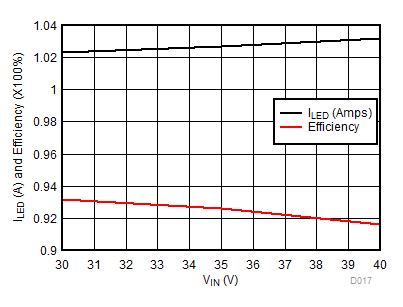
| VLED = 13 V | VIADJ=2.4 V | RSENSE = 0.196 Ω |