ZHCSFD3A April 2016 – August 2016 TPS92515 , TPS92515-Q1 , TPS92515HV , TPS92515HV-Q1
PRODUCTION DATA.
- 1 特性
- 2 应用
- 3 说明
- 4 修订历史记录
- 5 Device Comparison Table
- 6 Pin Configuration and Functions
- 7 Specifications
-
8 Detailed Description
- 8.1 Overview
- 8.2 Functional Block Diagram
- 8.3
Feature Description
- 8.3.1 General Operation
- 8.3.2 Current Sense Comparator
- 8.3.3 OFF Timer
- 8.3.4 OFF-Timer, Shunt FET Dimming or Shunted Output Condition
- 8.3.5 Internal N-channel MOSFET
- 8.3.6 VCC Internal Regulator and Undervoltage Lockout (UVLO)
- 8.3.7 Analog Adjust Input
- 8.3.8 Thermal Protection
- 8.3.9 Junction Temperature Relative Estimation
- 8.3.10 BOOT and BOOT UVLO
- 8.3.11 PWM (UVLO and Enable)
- 8.4 Device Functional Modes
-
9 Application and Implementation
- 9.1 Application Information
- 9.2
Typical Application
- 9.2.1 General Design Procedure
- 9.2.2 Design Requirements
- 9.2.3
Detailed Design Procedure
- 9.2.3.1 Calculating Duty Cycle
- 9.2.3.2 Calculate OFF-Time Estimate
- 9.2.3.3 Calculate OFF-Time Resistor ROFF
- 9.2.3.4 Calculate the Inductance Value
- 9.2.3.5 Calculate the Sense Resistance
- 9.2.3.6 Calculate Input Capacitance
- 9.2.3.7 Verify Peak Current for Inductor Selection
- 9.2.3.8 Calculate Output Capacitance
- 9.2.3.9 Calculate UVLO Resistance Values
- 9.2.4 Application Curves
- 9.3 Dos and Don'ts
- 10Power Supply Recommendations
- 11Layout
- 12器件和文档支持
- 13机械、封装和可订购信息
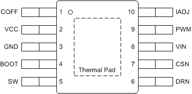
6 Pin Configuration and Functions
DGQ Package
HVSSOP 10-Pin with PowerPAD
Top View

Pin Functions
| PIN | I/O | DESCRIPTION | |
|---|---|---|---|
| NAME | NO. | ||
| BOOT | 4 | I | Connect a ceramic capacitor between BOOT and SW and a diode from VCC to BOOT to power the high-side FET drive circuitry. |
| COFF | 1 | I | Connect a resistor from VOUT, and a capacitor to GND to set the OFF-time. |
| CSN | 7 | I | Current sense negative input. Connect current sense resistor from VIN to CSN for high-side current sense control. |
| DRN | 6 | I | Internal FET drain. Connect to CSN node |
| GND | 3 | G | Ground |
| IADJ | 10 | I | Output current adjust. Connect to an external divider, reference or tie to VCC. |
| PWM | 9 | I | PWM dimming input. Connect to PWM control signal. Output current is pulse-width modulated (PWM) dimmed from the maximum analog controlled level. Connect to VCC if not used. |
| SW | 5 | O | Internal FET Source. Connect to output inductor |
| VCC | 2 | O | 5-V Regulator Output. Use a decoupling capacitor from VCC to ground. See section on VCC capacitor selection. |
| VIN | 8 | I | Connect to input voltage. VIN is also the current sense positive input. |
| Thermal pad | — | Connect to ground | |