ZHCSGH9 June 2017 TPS7A90
PRODUCTION DATA.
- 1 特性
- 2 应用
- 3 说明
- 4 修订历史记录
- 5 Pin Configuration and Functions
- 6 Specifications
-
7 Detailed Description
- 7.1 Overview
- 7.2 Functional Block Diagram
- 7.3 Feature Description
- 7.4 Device Functional Modes
- 8 Application and Implementation
- 9 Power Supply Recommendations
- 10Layout
- 11器件和文档支持
- 12机械、封装和可订购信息
7 Detailed Description
7.1 Overview
The TPS7A90 is a low-noise, high PSRR, low dropout (LDO) regulator capable of sourcing a 500-mA load with only 200 mV of maximum dropout. The TPS7A90 can operate down to a 1.4-V input voltage and a 0.8-V output voltage. This combination of low-noise, high PSRR, and low dropout voltage makes the device an ideal LDO to power a multitude of loads from noise-sensitive communication components in high-speed communications applications to high-end microprocessors or field-programmable gate arrays (FPGAs).
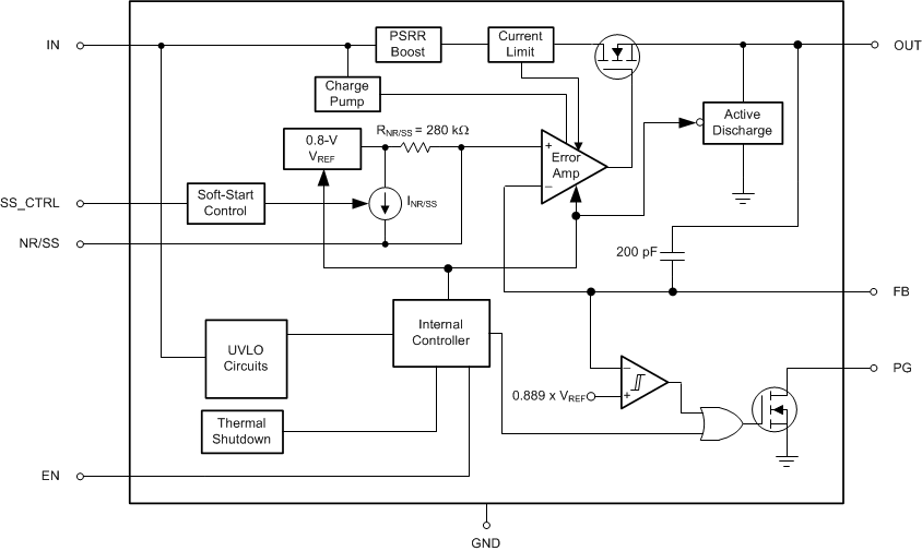
As shown in the Functional Block Diagram section, the TPS7A90 linear regulator features a low-noise, 0.8-V internal reference that can be filtered externally to obtain even lower output noise. The internal protection circuitry (such as the undervoltage lockout) prevents the device from turning on before the input is high enough to ensure accurate regulation. Foldback current limiting is also included, allowing the output to source the rated output current when the output voltage is in regulation but reduces the allowable output current during short-circuit conditions. The internal power-good detection circuit allows down-stream supplies to be sequenced and alerts if the output voltage is below a regulation threshold.
7.2 Functional Block Diagram

7.3 Feature Description
7.3.1 Output Enable
The enable pin (EN) for the TPS7A90 is active high. The output voltage is enabled when the enable pin voltage is greater than VIH(EN) and disabled with the enable pin voltage is less than VIL(EN). If independent control of the output voltage is not needed, then connect the enable pin to the input.
The TPS7A90 has an internal pulldown MOSFET that connects a discharge resistor from VOUT to ground when the device is disabled to actively discharge the output voltage.
7.3.2 Dropout Voltage (VDO)
Dropout voltage (VDO) is defined as the VIN – VOUT voltage at the rated current (IRATED) of 500 mA, where the pass-FET is fully on and in the ohmic region of operation. VDO indirectly specifies a minimum input voltage above the nominal programmed output voltage at which the output voltage is expected to remain in regulation. If the input falls below the nominal output regulation, then the output follows the input.
Dropout voltage is determined by the RDS(ON) of the pass-FET. Therefore, if the LDO operates below the rated current, then the VDO for that current scales accordingly. Use Equation 1 to calculate the RDS(ON) for the TPS7A90:

7.3.3 Output Voltage Accuracy
Output voltage accuracy specifies minimum and maximum output voltage error, relative to the expected nominal output voltage stated as a percent. The TPS7A90 features an output voltage accuracy of 1% that includes the errors introduced by the internal reference, load regulation, and line regulation variance across the full range of rated load and line operating conditions over temperature, as specified by the Electrical Characteristics table. Output voltage accuracy also accounts for all variations between manufacturing lots.
7.3.4 High Power-Supply Rejection Ratio (PSRR)
PSRR is a measure of how well the LDO control loop rejects noise from the input source to make the dc output voltage as noise-free as possible across the frequency spectrum (usually measured from 10 Hz to 10 MHz). Even though PSRR is a loss in noise signal amplitude, the PSRR curves in the Typical Characteristics section are illustrated as positive values in decibels (dB) for convenience. Equation 2 gives the PSRR calculation as a function of frequency where input noise voltage [VIN(f)] and output noise voltage [VOUT(f)] are the amplitudes of the respective sinusoidal signals.

Noise that couples from the input to the internal reference voltage is a primary contributor to reduced PSRR performance. Using a noise-reduction capacitor is recommended to filter unwanted noise from the input voltage, which creates a low-pass filter with an internal resistor to improve PSRR performance at lower frequencies.
LDOs are often employed not only as a step-down regulators, but also to provide exceptionally clean power rails for noise-sensitive components. This usage is especially true for the TPS7A90, which features an innovative circuit to boost the PSRR between 200 kHz and 1 MHz. This boost circuit helps further filter switching noise from switching-regulators that operate in this region; see Figure 1. To achieve the maximum benefit of this PSRR boost circuit, using a capacitor with a minimum impedance in the 100-kHz to 1-MHz band is recommended.
7.3.5 Low Output Noise
LDO noise is defined as the internally-generated intrinsic noise created by the semiconductor circuits. The TPS7A90 is designed for system applications where minimizing noise on the power-supply rail is critical to system performance. This scenario is the case for phase-locked loop (PLL)-based clocking circuits where minimum phase noise is all important, or in test and measurement systems where even small power-supply noise fluctuations can distort instantaneous measurement accuracy.
The TPS7A90 includes a low-noise reference ensuring minimal output noise in normal operation. Further improvements can be made by adding a noise-reduction capacitor (CNR/SS), a feedforward capacitor (CFF), or a combination of the two. See the Noise-Reduction and Soft-Start Capacitor (CNR/SS) and Feed-Forward Capacitor (CFF) sections for additional design information.
For more information on noise and noise measurement, see the How to Measure LDO Noise white paper.
7.3.6 Output Soft-Start Control
Soft-start refers to the ramp-up characteristic of the output voltage during LDO turn-on after the EN and UVLO thresholds are exceeded. The noise-reduction capacitor (CNR/SS) serves a dual purpose of both governing output noise reduction and programming the soft-start ramp during turn-on. Larger values for the noise-reduction capacitors decrease the noise but also result in a slower output turn-on ramp rate.
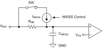
The TPS7A90 features an SS_CTRL pin. When the SS_CTRL pin is grounded, the charging current for the NR/SS pin is 6.2 µA (typ); when this pin is connected to IN, the charging current for the NR/SS pin is increased to 100 µA (typ). The higher current allows the use of a much larger noise-reduction capacitor and maintains a reasonable startup time. Figure 36 shows a simplified block diagram of the soft-start circuit. The switch SW is opened to turn off the INR/SS current source after VFB reaches approximately 97% of VREF. The final 3% of VNR/SS is charged through the noise-reduction resistor (RNR), which creates an RC delay. RNR is approximately 280 kΩ and applications that require the highest accuracy when using a large value CNR/SS must take this RC delay into account.
If a noise-reduction capacitor is not used on the NR/SS pin, tying the SS_CTRL pin to the IN pin can result in output voltage overshoot of approximately 10%. This overshoot is minimized by either connecting the SS_CTRL pin to GND or using a capacitor on the NR/SS pin.
 Figure 36. Simplified Soft-Start Circuit
7.3.7 Power-Good Function
The power-good circuit monitors the voltage at the feedback pin to indicate the status of the output voltage. When the feedback pin voltage falls below the PG threshold voltage (VIT(PG)), the PG pin open-drain output engages and pulls the PG pin close to GND. When the feedback voltage exceeds the VIT(PG) threshold by an amount greater than VHYS(PG), the PG pin becomes high impedance. By connecting a pullup resistor to an external supply, any downstream device can receive power-good as a logic signal that can be used for sequencing. Make sure that the external pullup supply voltage results in a valid logic signal for the receiving device or devices. Using a pullup resistor from 10 kΩ to 100 kΩ is recommended. Using an external reset device such as the TPS3890 is also recommended in applications where high accuracy is needed or in applications where microprocessor induced resets are needed.
When using a feed-forward capacitor (CFF), the time constant for the LDO startup is increased whereas the power-good output time constant stays the same, possibly resulting in an invalid status of the power-good output. To avoid this issue and to receive a valid PG output, make sure that the time constant of both the LDO startup and the power-good output are matching, which can be done by adding a capacitor in parallel with the power-good pullup resistor. For more information, see the application report Pros and Cons of Using a Feedforward Capacitor with a Low-Dropout Regulator.
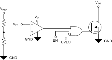
The state of PG is only valid when the device is operating above the minimum input voltage of the device and power-good is asserted regardless of the output voltage state when the input voltage falls below the UVLO threshold minus the UVLO hysteresis. Figure 37 illustrates a simplified block diagram of the power-good circuit. When the input voltage falls below approximately 0.8 V, there is not enough gate drive voltage to keep the open-drain, power-good device turned on and the power-good output is pulled high. Connecting the power-good pullup resistor to the output voltage can help minimize this effect.
 Figure 37. Simplified PG Circuit
7.3.8 Internal Protection Circuitry
7.3.8.1 Undervoltage Lockout (UVLO)
The TPS7A90 has an independent undervoltage lockout (UVLO) circuit that monitors the input voltage, allowing a controlled and consistent turn on and off of the output voltage. To prevent the device from turning off if the input drops during turn on, the UVLO has approximately 290 mV of hysteresis.
The UVLO circuit responds quickly to glitches on VIN and disables the output of the device if this rail starts to collapse too quickly. Use an input capacitor that is large enough to slow input transients to less then two volts per microsecond.
7.3.8.2 Internal Current Limit (ICL)
The internal current-limit circuit is used to protect the LDO against transient high-load current faults or shorting events. The LDO is not designed to operate in current limit under steady-state conditions. During an overcurrent event where the output voltage is pulled 10% below the regulated output voltage, the LDO sources a constant current as specified in the Electrical Characteristics table. When the output voltage falls, the amount of output current is reduced to better protect the device. During a hard short-circuit event, the current is reduced to approximately 1.45 A. See Figure 12 in the Typical Characteristics section for more information about the current-limit foldback behavior. However, when a current-limit event occurs, the LDO begins to heat up because of the increase in power dissipation. The increase in heat can trigger the integrated thermal shutdown protection circuit.
7.3.8.3 Thermal Protection
The TPS7A90 contains a thermal shutdown protection circuit to turn off the output current when excessive heat is dissipated in the LDO. Thermal shutdown occurs when the thermal junction temperature (TJ) of the pass-FET exceeds 160°C (typical). Thermal shutdown hysteresis assures that the LDO again resets (turns on) when the temperature falls to 140°C (typical). The thermal time-constant of the semiconductor die is fairly short, and thus the output turns on and off at a high rate when thermal shutdown is reached until power dissipation is reduced.
The internal protection circuitry of the TPS7A90 is designed to protect against thermal overload conditions. The circuitry is not intended to replace proper heat sinking. Continuously running the TPS7A90 into thermal shutdown degrades device reliability.
For reliable operation, limit junction temperature to a maximum of 125°C. To estimate the thermal margin in a given layout, increase the ambient temperature until the thermal protection shutdown is triggered using worst-case load and highest input voltage conditions. For good reliability, thermal shutdown must occur at least 35°C above the maximum expected ambient temperature condition for the application. This configuration produces a worst-case junction temperature of 125°C at the highest expected ambient temperature and worst-case load.
7.4 Device Functional Modes
Table 1 provides a quick comparison between the normal, dropout, and disabled modes of operation.
Table 1. Device Functional Modes Comparison
| OPERATING MODE | PARAMETER | |||
|---|---|---|---|---|
| VIN | EN | IOUT | TJ | |
| Normal(1) | VIN > VOUT(nom) + VDO | VEN > VIH(EN) | IOUT < ICL | TJ < Tsd |
| Dropout(1) | VIN < VOUT(nom) + VDO | VEN > VIH(EN) | IOUT < ICL | TJ < Tsd |
| Disabled(2) | VIN < VUVLO | VEN < VIL(EN) | — | TJ > Tsd |
7.4.1 Normal Operation
The device regulates to the nominal output voltage when all of the following conditions are met:
- The input voltage is greater than the nominal output voltage plus the dropout voltage (VOUT(nom) + VDO)
- The enable voltage has previously exceeded the enable rising threshold voltage and has not yet decreased below the enable falling threshold
- The output current is less than the current limit (IOUT < ICL)
- The device junction temperature is less than the thermal shutdown temperature (TJ < Tsd)
7.4.2 Dropout Operation
If the input voltage is lower than the nominal output voltage plus the specified dropout voltage, but all other conditions are met for normal operation, the device operates in dropout. In this mode, the output voltage tracks the input voltage. During this mode, the transient performance of the device becomes significantly degraded because the pass device is in a triode state and no longer controls the current through the LDO. Line or load transients in dropout can result in large output-voltage deviations.
When the device is in a steady dropout state (defined as when the device is in dropout, VIN < VOUT(NOM) + VDO, right after being in a normal regulation state, but not during startup), the pass-FET is driven as hard as possible. When the input voltage returns to VIN ≥ VOUT(NOM) + VDO, VOUT can overshoot for a short period of time if the input voltage slew rate is greater than 0.1 V/µs.
7.4.3 Disabled
The output of the TPS7A90 can be shutdown by forcing the enable pin below 0.4 V. When disabled, the pass device is turned off, internal circuits are shutdown, and the output voltage is actively discharged to ground by an internal resistor from the output to ground.