ZHCSGH9 June 2017 TPS7A90
PRODUCTION DATA.
- 1 特性
- 2 应用
- 3 说明
- 4 修订历史记录
- 5 Pin Configuration and Functions
- 6 Specifications
-
7 Detailed Description
- 7.1 Overview
- 7.2 Functional Block Diagram
- 7.3 Feature Description
- 7.4 Device Functional Modes
- 8 Application and Implementation
- 9 Power Supply Recommendations
- 10Layout
- 11器件和文档支持
- 12机械、封装和可订购信息
6 Specifications
6.1 Absolute Maximum Ratings
over operating junction temperature range and all voltages with respect to GND (unless otherwise noted)(1)| MIN | MAX | UNIT | ||
|---|---|---|---|---|
| Voltage | IN, PG, EN | –0.3 | 7.0 | V |
| IN, PG, EN (5% duty cycle, pulse duration ≤ 200 µs) | –0.3 | 7.5 | ||
| OUT | –0.3 | VIN + 0.3 | ||
| SS_CTRL | –0.3 | VIN + 0.3 | ||
| NR/SS, FB | –0.3 | 3.6 | ||
| Current | OUT | Internally limited | A | |
| PG (sink current into the device) | 5 | mA | ||
| Temperature | Operating junction, TJ | –55 | 150 | °C |
| Storage, Tstg | –55 | 150 | °C | |
(1) Stresses beyond those listed under Absolute Maximum Ratings may cause permanent damage to the device. These are stress ratings only, which do not imply functional operation of the device at these or any other conditions beyond those indicated under Recommended Operating Conditions. Exposure to absolute-maximum-rated conditions for extended periods may affect device reliability.
6.2 ESD Ratings
| VALUE | UNIT | |||
|---|---|---|---|---|
| V(ESD) | Electrostatic discharge | Human body model (HBM), per ANSI/ESDA/JEDEC JS-001(1) | ±2000 | V |
| Charged device model (CDM), per JEDEC specification JESD22-C101(2) | ±500 | |||
(1) JEDEC document JEP155 states that 500-V HBM allows safe manufacturing with a standard ESD control process.
(2) JEDEC document JEP157 states that 250-V CDM allows safe manufacturing with a standard ESD control process.
6.3 Recommended Operating Conditions
over operating junction temperature range (unless otherwise noted)| MIN | MAX | UNIT | ||
|---|---|---|---|---|
| VIN | Input supply voltage range | 1.4 | 6.5 | V |
| VOUT | Output voltage range | 0.8 | 5.7 | V |
| IOUT | Output current | 0 | 0.5 | A |
| CIN | Input capacitor | 10 | µF | |
| COUT | Output capacitor | 10 | µF | |
| CNR/SS | Noise-reduction capacitor | 0 | 10 | µF |
| CFF | Feedforward capacitor | 0 | 100 | nF |
| RPG | Power-good pullup resistance | 10 | 100 | kΩ |
| TJ | Junction temperature | –40 | 125 | °C |
6.4 Thermal Information
| THERMAL METRIC(1) | TPS7A90 | UNIT | |
|---|---|---|---|
| DSK (SON) | |||
| 10 PINS | |||
| RθJA | Junction-to-ambient thermal resistance | 56.9 | °C/W |
| RθJC(top) | Junction-to-case (top) thermal resistance | 46.3 | °C/W |
| RθJB | Junction-to-board thermal resistance | 29.1 | °C/W |
| ψJT | Junction-to-top characterization parameter | 0.8 | °C/W |
| ψJB | Junction-to-board characterization parameter | 29.4 | °C/W |
| RθJC(bot) | Junction-to-case (bottom) thermal resistance | 3.2 | °C/W |
(1) For more information about traditional and new thermal metrics, see the Semiconductor and IC Package Thermal Metrics application report.
6.5 Electrical Characteristics
over operating temperature range (TJ = –40°C to +125°C), 1.4 V ≤ VIN ≤ 6.5 V, VOUT(NOM) = 0.8 V, IOUT = 5 mA, VEN = 1.4 V, CIN = COUT = 10 μF, CNR/SS = CFF = 0 nF, SS_CTRL = GND, and PG pin pulled up to VIN with 100 kΩ (unless otherwise noted); typical values are at TJ = 25°C| PARAMETER | TEST CONDITIONS | MIN | TYP | MAX | UNIT | |
|---|---|---|---|---|---|---|
| VIN | Input supply voltage range | 1.4 | 6.5 | V | ||
| VREF | Reference voltage | 0.8 | V | |||
| VUVLO | Input supply UVLO | VIN rising | 1.31 | 1.39 | V | |
| VHYS(UVLO) | Input supply UVLO hysteresis | 290 | mV | |||
| VOUT | Output voltage range | 0.8 | 5.7 | V | ||
| Output voltage accuracy(1) | 1.4 V ≤ VIN ≤ 6.5 V, 5 mA ≤ IOUT ≤ 0.5 A | –1.0% | 1.0% | |||
| ΔVOUT(ΔVIN) | Line regulation | 0.005 | %/V | |||
| ΔVOUT(ΔIOUT) | Load regulation(2) | 5 mA ≤ IOUT ≤ 0.5 A | 0.02 | %/A | ||
| VDO | Dropout voltage | 1.4 V ≤ VIN ≤ 5.0 V, IOUT = 0.5 A, VFB = 0.8 V – 3% | 100 | mV | ||
| 5.0 V < VIN ≤ 5.7 V, IOUT = 0.5 A, VFB = 0.8 V – 3% | 200 | |||||
| ILIM | Output current limit | VOUT forced at 0.9 × VOUT(NOM), VIN = VOUT(NOM) + 300 mV |
0.8 | 1.1 | 1.5 | A |
| IGND | GND pin current | VIN = 6.5 V, IOUT = 5 mA | 2.1 | 3.5 | mA | |
| VIN = 1.4 V, IOUT = 0.5 A | 4 | |||||
| ISDN | Shutdown GND pin current | PG = (open), VIN = 6.5 V, VEN = 0.4 V | 0.1 | 15 | µA | |
| IEN | EN pin current | VIN = 6.5 V, 0 V ≤ VEN ≤ 6.5 V | –0.2 | 0.2 | µA | |
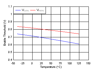
| VIL(EN) | EN pin low-level input voltage (device disabled) | 0 | 0.4 | V | ||
| VIH(EN) | EN pin high-level input voltage (device enabled) | 1.1 | 6.5 | V | ||
| ISS_CTRL | SS_CTRL pin current | VIN = 6.5 V, 0 V ≤ VSS_CTRL ≤ 6.5 V | –0.2 | 0.2 | µA | |
| VIT(PG) | PG pin threshold | For PG transitioning low with falling VOUT, expressed as a percentage of VOUT(NOM) | 82% | 88.9% | 93% | |
| VHYS(PG) | PG pin hysteresis | For PG transitioning high with rising VOUT, expressed as a percentage of VOUT(NOM) | 1% | |||
| VOL(PG) | PG pin low-level output voltage | VOUT < VIT(PG), IPG = –1 mA (current into device) | 0.4 | V | ||
| ILKG(PG) | PG pin leakage current | VOUT > VIT(PG), VPG = 6.5 V | 1 | µA | ||
| INR/SS | NR/SS pin charging current | VNR/SS = GND, VSS_CTRL = GND | 4.0 | 6.2 | 9.0 | µA |
| VNR/SS = GND, VSS_CTRL = VIN | 65 | 100 | 150 | |||
| IFB | FB pin leakage current | VIN = 6.5 V, VFB = 0.8 V | –100 | 100 | nA | |
| PSRR | Power-supply ripple rejection | f = 500 kHz, VIN = 3.8 V, VOUT(NOM) = 3.3 V, IOUT = 250mA, CNR/SS = 10 nF, CFF = 10 nF |
39 | dB | ||
| Vn | Output noise voltage | BW = 10 Hz to 100 kHz, VIN = 1.8 V, VOUT(NOM) = 0.8 V, IOUT = 0.5 A, CNR/SS = 10 nF, CFF = 10 nF |
4.7 | µVRMS | ||
| Noise spectral density | f = 10 kHz, VIN = 1.8 V, VOUT(NOM) = 0.8 V, IOUT = 0.5 A, CNR/SS = 10 nF, CFF = 10 nF |
13 | nV/√Hz | |||
| Rdiss | Output active discharge resistance | VEN = GND | 250 | Ω | ||
| Tsd | Thermal shutdown temperature | Shutdown, temperature increasing | 160 | °C | ||
| Reset, temperature decreasing | 140 | |||||
(1) When the device is connected to external feedback resistors at the FB pin, external resistor tolerances are not included.
(2) The device is not tested under conditions where VIN > VOUT + 2.5 V and IOUT = 0.5 A because the power dissipation is higher than the maximum rating of the package. Also, this accuracy specification does not apply on any application condition that exceeds the power dissipation limit of the package under test.
6.6 Typical Characteristics
at TJ = 25°C, 1.4 V ≤ VIN ≤ 6.5 V, VIN ≥ VOUT(NOM) + 0.3 V, VOUT = 0.8 V, SS_CTRL = GND, IOUT = 5 mA, VEN = 1.1 V, COUT = 10 μF, CNR/SS = CFF = 0 nF, PG pin pulled up to VOUT with 100 kΩ, and SS_CTRL = GND (unless otherwise noted)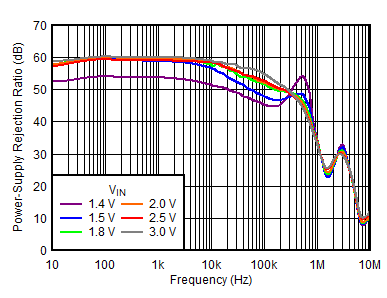
| VOUT = 0.8 V, IOUT = 500 mA, COUT = 10 µF, CNR/SS = CFF = 10 nF |
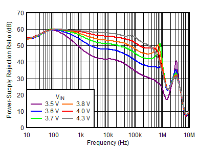
| VOUT = 3.3 V, IOUT = 500 mA, COUT = 10 µF, CNR/SS = CFF = 10 nF |
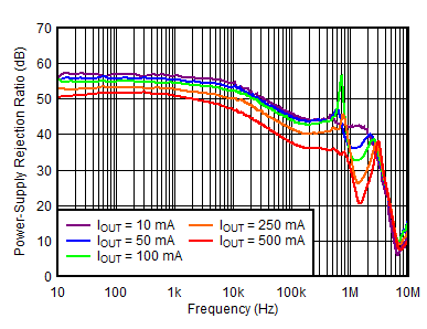
| VOUT = 1.2 V, VIN = VEN = 1.5 V, COUT = 10 µF, CNR/SS = CFF = 10 nF |
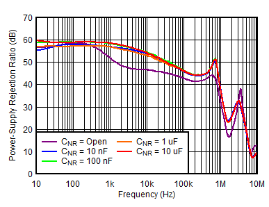
| VOUT = 1.2 V, VIN = VEN = 1.7 V, IOUT = 500 mA, COUT = 10 µF, CFF = 10 nF |
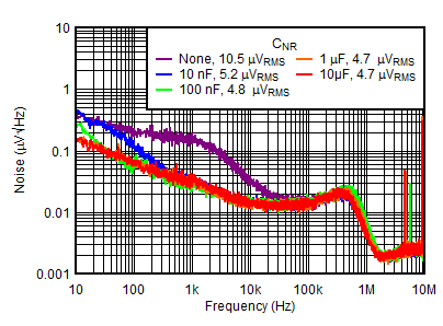
| VIN = 2.2 V, VOUT = 1.2 V, IOUT = 500 mA, CIN = COUT = 10 µF, CFF = 10 nF, VRMS BW = 10 Hz to 100 kHz |
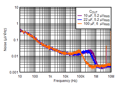
| VIN = 2.2 V, VOUT = 1.2 V, IOUT = 500 mA, CIN = 10 µF, CNR/SS = CFF = 10 nF, VRMS BW = 10 Hz to 100 kHz |
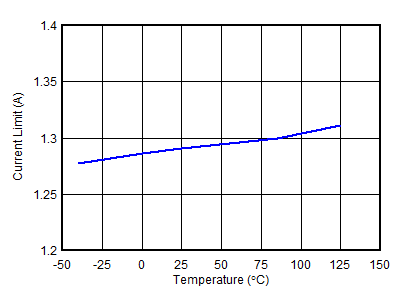
| VIN = 1.4 V, VOUT = 0.8 V |
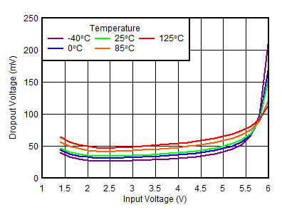
| IOUT = 500 mA |
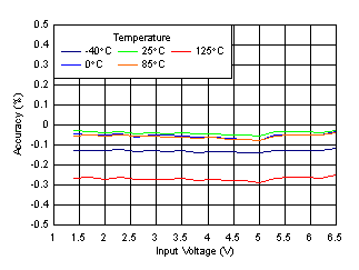
| IOUT = 50 mA |
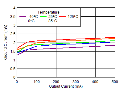
| VIN = 1.4 V |
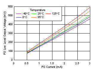
(VIN = 1.4 V)
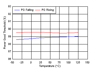
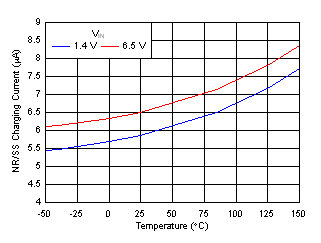
(SS_CTRL = GND)
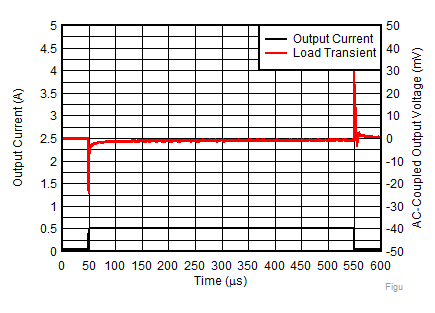
| VIN = 1.4 V, IOUT = 50 mA to 500 mA to 50 mA at 1 A/µs, COUT = 10 µF, VPG = VOUT |
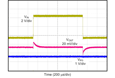
| VIN = 1.4 V to 6.5 V to 1.4 V at 2 V/µs, VOUT = 0.8 V, IOUT = 500 mA, CNR/SS = CFF = 10 nF, VPG = VOUT |
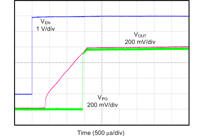
| VIN = 1.4 V, VPG = VOUT |
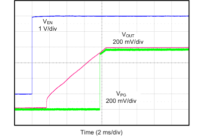
| VIN = 1.4 V, VPG = VOUT |
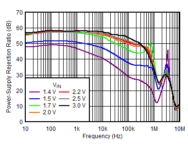
| VOUT = 1.2 V, IOUT = 500 mA, COUT = 10 µF, CNR/SS = CFF = 10 nF |
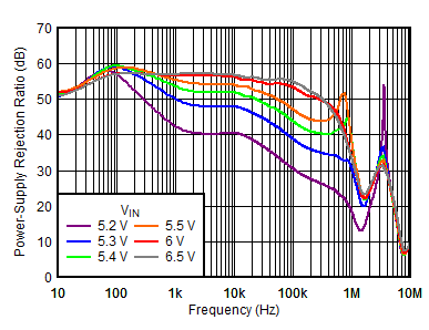
| VOUT = 5 V, IOUT = 500 mA, COUT = 10 µF, CNR/SS = CFF = 10 nF |
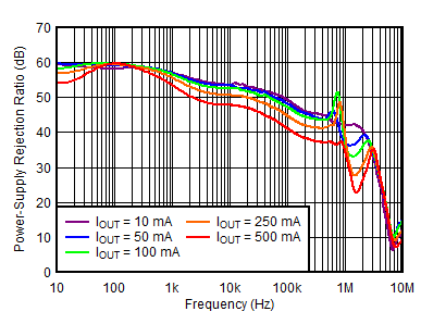
| VOUT = 3.3 V, VIN = VEN = 3.6 V, COUT = 10 µF, CNR/SS = CFF = 10 nF |
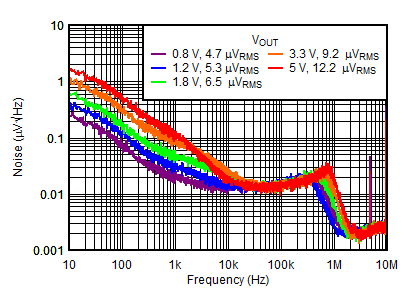
| VIN = VOUT + 1.0 V, IOUT = 500 mA, CIN = COUT = 10 µF, CNR/SS = CFF = 10 nF, VRMS BW = 10 Hz to 100 kHz |
Output Voltage
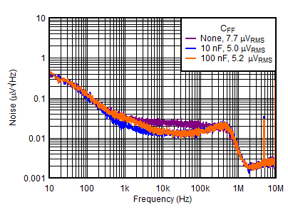
| VIN = 2.2 V, VOUT = 1.2 V, IOUT = 500 mA, CIN = COUT = 10 µF, CNR/SS = 10 nF, VRMS BW = 10 Hz to 100 kHz |
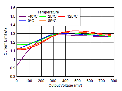
| VIN = 1.4 V, VOUT = 0.8 V | ||
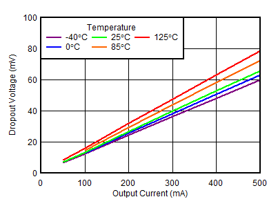
| VIN = 5.5 V |
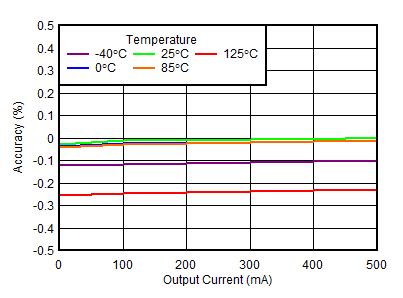
| VIN = 1.4 V |
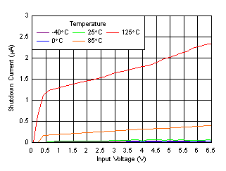
| VEN = 0.4 V |
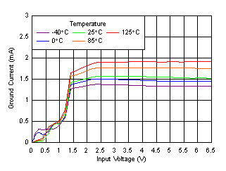
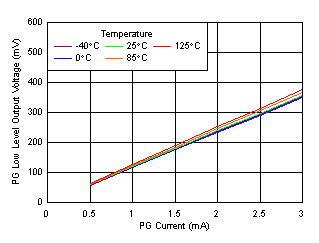
(VIN = 6.5 V)
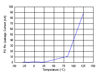
| VIN = VPG = 6.5 V |
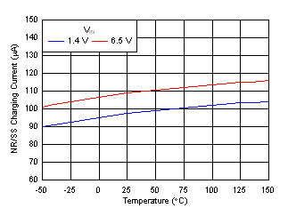
(SS_CTRL = VIN)
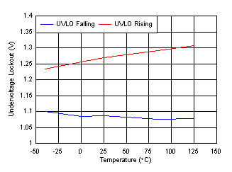
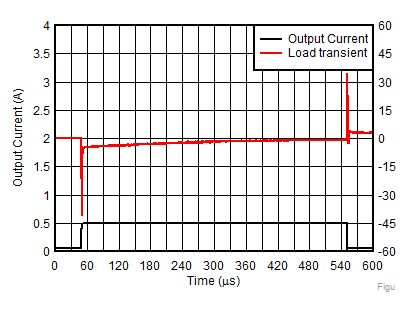
| VIN = 5.5 V, IOUT = 50 mA to 500 mA to 50 mA at 1 A/µs, COUT = 10 µF, VPG = VOUT |
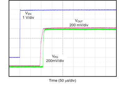
| VIN = 1.4 V, VPG = VOUT | ||
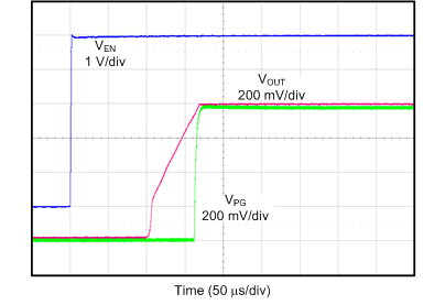
| VIN = 1.4 V, VPG = VOUT |