SLVSC31D December 2013 – August 2015 TPS7A4501-SP
PRODUCTION DATA.
- 1 Features
- 2 Applications
- 3 Description
- 4 Revision History
- 5 Description (continued)
- 6 Pin Configuration and Functions
- 7 Specifications
- 8 Detailed Description
- 9 Application and Implementation
- 10Power Supply Recommendations
- 11Layout
- 12Device and Documentation Support
- 13Mechanical, Packaging, and Orderable Information
封装选项
机械数据 (封装 | 引脚)
散热焊盘机械数据 (封装 | 引脚)
订购信息
9 Application and Implementation
NOTE
Information in the following applications sections is not part of the TI component specification, and TI does not warrant its accuracy or completeness. TI’s customers are responsible for determining suitability of components for their purposes. Customers should validate and test their design implementation to confirm system functionality.
9.1 Application Information
The TPS7A4501-SP regulator has very-low output noise, which makes it ideal for sensitive RF supply applications.
9.2 Typical Application
This section highlights some of the design considerations when implementing this device in various applications.
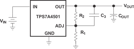
 Figure 23. Adjustable Output Voltage Operation
9.2.1 Design Requirements
Table 2 shows the design requirements.
Table 2. Design Parameters
| DESIGN PARAMETER | EXAMPLE VALUE |
|---|---|
| Input voltage (VIN) | 5 V |
| Output voltage (VOUT) | 2.5 V |
| Output current (IOUT) | 0 to 1 A |
| Load regulation | 1% |
9.2.2 Detailed Design Procedure
The TPS7A4501-SP has an adjustable output voltage range of 1.21 to 20 V. The output voltage is set by the ratio of two external resistors, R1 and R2, as shown in Figure 23. The device maintains the voltage at the ADJ pin at 1.21 V referenced to ground. The current in R1 is then equal to (1.21 V/R1), and the current in R2 is the current in R1 plus the ADJ pin bias current. The ADJ pin bias current, 3 µA at 25°C, flows through R2 into the ADJ pin. Calculate the output voltage using Equation 2.

The value of R1 should be less than 4.17 kΩ to minimize errors in the output voltage caused by the ADJ pin bias current. Note that in shutdown the output is turned off, and the divider current is zero. For an output voltage of 2.50 V, R1 is set to 4 kΩ. R2 is then found to be 4.22 kΩ using Equation 2.

The adjustable device is tested and specified with the ADJ pin tied to the OUT pin for an output voltage of 1.21 V. Specifications for output voltages greater than 1.21 V are proportional to the ratio of the desired output voltage to 1.21 V: VOUT / 1.21 V. For example, load regulation for an output current change of 1 mA to 1.5 A is –2 mV (typical) at VOUT = 1.21 V. At VOUT = 2.50 V, the typical load regulation is:
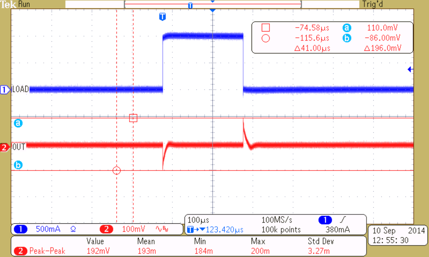
shows the actual change in output is about 3 mV for a 1-A load step. The maximum load regulation at 25°C is –8 mV. At VOUT = 2.50 V, the maximum load regulation is:
Because 16.53 mV is only 0.7% of the 2.5-V output voltage, the load regulation meets the design requirements.
9.2.2.1 Output Capacitance and Transient Response
The TPS7A4501-SP regulator is designed to be stable with a wide range of output capacitors. The ESR of the output capacitor affects stability, most notably with small capacitors. TI recommends a minimum output capacitor of 10 μF with an ESR of 3 Ω or less to prevent oscillations. Larger values of output capacitance can decrease the peak deviations and provide improved transient response for larger load current changes. Bypass capacitors, used to decouple individual components powered by the TPS7A4501-SP, increase the effective output capacitor value.
Give extra consideration to the use of ceramic capacitors. Ceramic capacitors are manufactured with a variety of dielectrics, each with different behavior over temperature and applied voltage. The most common dielectric used for a harsh environment is X7R. Ceramic capacitors lose capacitance when DC bias is applied across the capacitor. This capacitance loss is due to the polarization of the ceramic material. The capacitance loss is not permanent: after a large DC bias is applied, reducing the DC bias reduces the degree of polarization and capacitance increases. DC bias effects vary dramatically with voltage rating, case size, capacitor value, and capacitor manufacturer. Because a capacitor could lose more than 50% of its capacitance with DC bias voltages near the voltage rating of the capacitor, it is important to consider DC bias when selecting a ceramic capacitor for an application.
Ceramic capacitors' dielectric also changes over the temperature range. For example X7R, the first letter X denotes lower temperature range –55°C whereas 7 denotes a higher temperature range 125°C and R denotes capacitance variation over the temperature range (±15%). For harsh environment applications, minimum dielectric thickness must be 1 mil for 100-V DC-rated capacitor and 0.8 mil for 50-V DC-rated capacitors.
Voltage and temperature coefficients are not the only sources of problems. Some ceramic capacitors have a piezoelectric response. A piezoelectric device generates voltage across its terminals due to mechanical stress, similar to the way a piezoelectric accelerometer or microphone works. For a ceramic capacitor, the stress can be induced by vibrations in the system or thermal transients.
Tantalum capacitors can provide higher capacitance per unit volume. Tantalum capacitors can be either manganese dioxide (MNO2)-based capacitors where the cathode is MN02 or polymer. MN02-based tantalum capacitors exhibit high ESR as compared to polymer-based tantalum capacitors. MN02-based tantalum capacitors require in excess of 60% voltage derating. Thus, a 10-V rated capacitor can only be used for 3.3-V application. Whereas polymer-based capacitors only require 10% voltage derating. Paralleling ceramic and tantalum capacitors provide optimum balance between capacitance and ESR.
Table 3 highlights some of the capacitors used in the device.
Table 3. TPS7A4501-SP Capacitors
| CAPACITOR PART NUMBER | CAPACITOR DETAILS TYPE VENDOR (CAPACITOR, VOLTAGE, ESR) |
TYPE | VENDOR |
|---|---|---|---|
| T493X226M025AH6x20 | 22 μF, 25 V, 35 mΩ | Tantalum - MnO2 | Kemet |
| T525D476M016ATE035 | 47 μF, 10 V, 35 mΩ | Tantalum - Polymer | Kemet |
| T525D107M010ATE025 | 100 μF, 10 V, 25 mΩ | Tantalum - Polymer | Kemet |
| T541X337M010AH6720 | 330 μF, 10 V, 6 mΩ | Tantalum - Polymer | Kemet |
| T525D227M010ATE025 | 220 μF, 10 V, 25 mΩ | Tantalum - Polymer | Kemet |
| T495X107K016ATE100 | 100 μF, 16 V, 100 mΩ | Tantalum - MnO2 | Kemet |
| CWR29FK227JTHC | 220 μF, 10 V, 180 mΩ | Tantalum - MnO2 | AVX |
| THJE107K016AJH | 100 μF, 16 V, 58 mΩ | Tantalum | AVX |
| THJE227K010AJH | 220 μF, 10 V, 40 mΩ | Tantalum | AVX |
| SR2225X7R335K1P5#M123 | 3.3 μF, 25 V, 10 mΩ | Ceramic | Presidio Components Inc |
9.2.2.2 Compensation
TPS7A4501-SP is internally compensated. However, the user can implement a lead network using C3 to boost the phase margin as well as reduce output noise.
 Figure 24. Compensation Schematic
R1, the bottom resistor, and R2, the top resistor, form the output voltage divider network. C3 across R2 adds a lead network.
For R1 = 3.2 kΩ and R2 = 10 kΩ, VOUT is set at 5 V and C3 = 470 pF.
Zero and pole can be calculated as shown in the following equations.


9.2.3 Application Curves
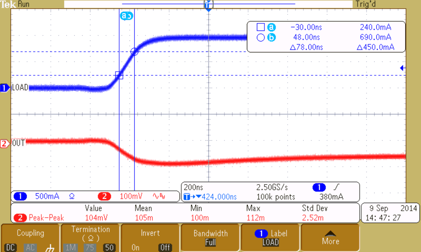
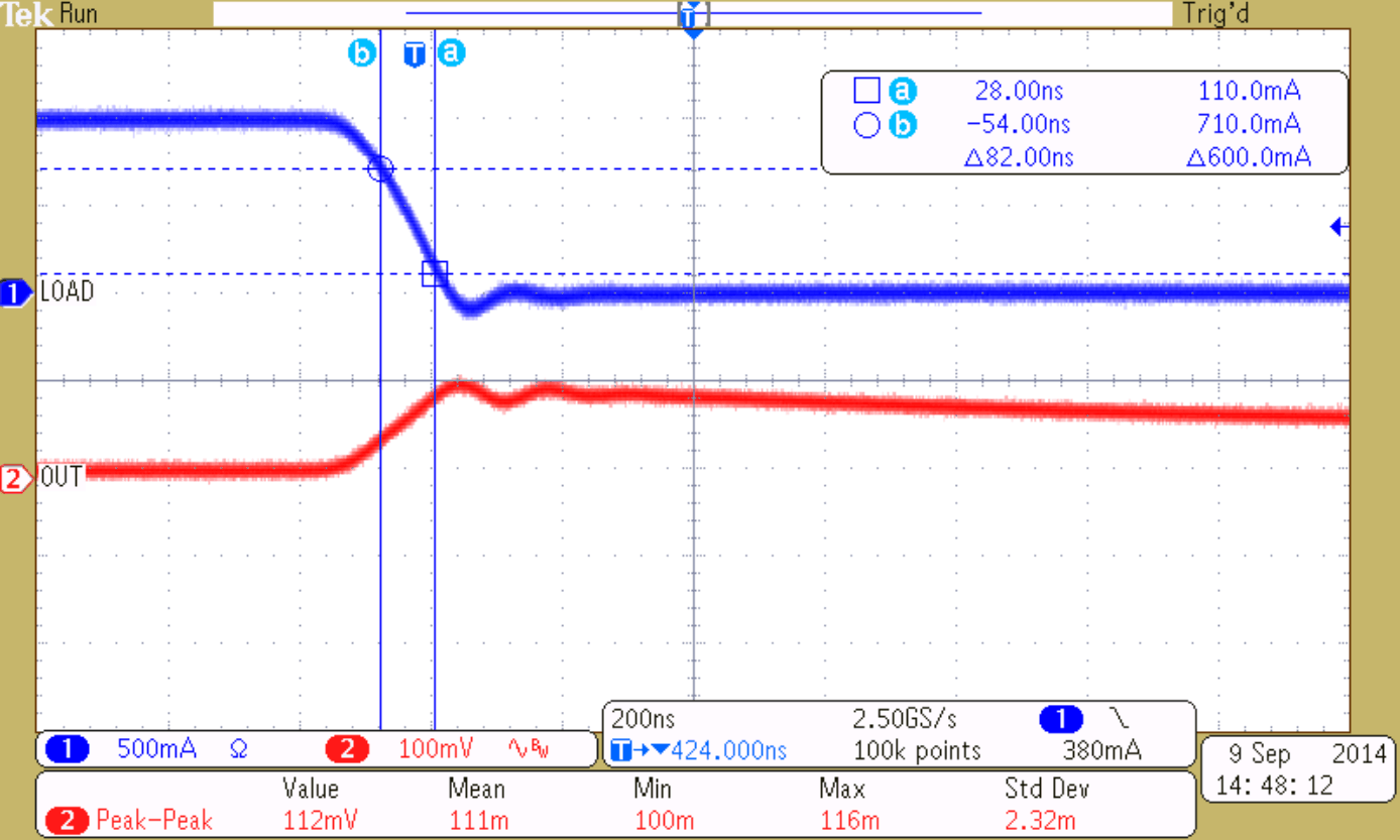
The following waveforms indicate the transient behavior of the TPS7A4501-SP.


