SLVSCK4A September 2015 – May 2016 TPS61235P , TPS61236P
PRODUCTION DATA.
- 1 Features
- 2 Applications
- 3 Description
- 4 Revision History
- 5 Device Comparison Table
- 6 Pin Configuration and Functions
- 7 Specifications
-
8 Detailed Description
- 8.1 Overview
- 8.2 Functional Block Diagram
- 8.3
Feature Description
- 8.3.1 Boost Controller Operation
- 8.3.2 Soft Start
- 8.3.3 Enable and Disable
- 8.3.4 Constant Output Voltage and Constant Output Current Operations
- 8.3.5 Over Current Protection
- 8.3.6 Load Status Indication
- 8.3.7 Under voltage Lockout
- 8.3.8 Over Voltage Protection and Reverse Current Block
- 8.3.9 Short Circuit Protection
- 8.3.10 Thermal Shutdown
- 8.4 Device Functional Modes
-
9 Applications and Implementation
- 9.1 Application Information
- 9.2
Typical Applications
- 9.2.1
TPS61236P 3-V to 4.35-V Input, 5-V Output Voltage, 3-A Maximum Output Current
- 9.2.1.1 Design Requirements
- 9.2.1.2 Detailed Design Procedure
- 9.2.1.3 TPS61236P 5-V Output Application Curves
- 9.2.2 TPS61236P 2.3-V to 5-V Input, 5-V 2-A Output Converter
- 9.2.1
TPS61236P 3-V to 4.35-V Input, 5-V Output Voltage, 3-A Maximum Output Current
- 10Power Supply Recommendations
- 11Layout
- 12Device and Documentation Support
- 13Mechanical, Packaging, and Orderable Information
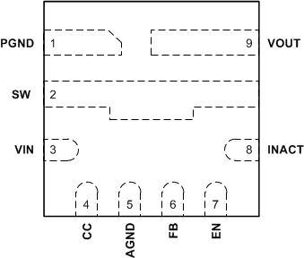
6 Pin Configuration and Functions
RWL Package
9-Pin VQFN
Top View

Pin Functions
| PIN | I/O | DESCRIPTION | |
|---|---|---|---|
| NAME | NUMBER | ||
| PGND | 1 | PWR | Power ground. |
| SW | 2 | PWR | The switch pin of the boost converter. It is connected to the drain of the internal Power MOSFETs. |
| VIN | 3 | I | IC power supply input. |
| CC | 4 | I | Constant output current programming pin. Connect a resistor to this pin to program the constant output current. A capacitor should be connected in parallel to stabilize the control loop. Connect this pin to the AGND pin to disable the constant output current function. |
| AGND | 5 | I/O | Analog ground. |
| FB | 6 | I | Voltage feedback pin of adjustable version (TPS61236P). Must be connected to VOUT pin on fixed output voltage version (TPS61235). |
| EN | 7 | I | Enable logic input. Logic high enables the device. Logic low disables the device and puts it in shutdown mode. This pin must be terminated and cannot be left floating. An external pull down resistor connected to this pin is recommended. |
| INACT | 8 | O | Load status indication. Open drain output. Can be left float or connected to AGND pin if not used. |
| VOUT | 9 | PWR | Boost converter output. |