SLVSE09A April 2017 – April 2017 TPS61096A
PRODUCTION DATA.
- 1 Features
- 2 Applications
- 3 Description
- 4 Revision History
- 5 Pin Configuration and Functions
- 6 Specifications
- 7 Detailed Description
- 8 Application and Implementation
- 9 Power Supply Recommendations
- 10Layout
- 11Device and Documentation Support
- 12Mechanical, Packaging, and Orderable Information
8 Application and Implementation
NOTE
Information in the following applications sections is not part of the TI component specification, and TI does not warrant its accuracy or completeness. TI’s customers are responsible for determining suitability of components for their purposes. Customers should validate and test their design implementation to confirm system functionality.
8.1 Application Information
The TPS61096A is a high output voltage boost converter with ultra-low quiescent current. It is designed for products powered by either two-cell alkaline, or one cell Li-Ion or Li-polymer battery, for which high efficiency under light load condition is critical to achieve long battery life operation. It can also support selective inductor peak current. With lower current limit, the TPS61096A can reduce inductor ripple so as to reduce external components size for light load applications. With higher current limit, the TPS61096A can have higher output current capability to meet more application requirements.
The TPS61096A integrates two-channel low-power level shifters to convert low level signals to output voltage signals for specific applications.
8.2 Typical Application
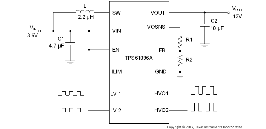 Figure 13. 12-V Pulse Generation From 3.6-V Input Voltage
8.2.1 Design Requirements
In this typical application, two channel 50-kHz pulse signals of 3.2 V amplitude are output from a controller, and the signals' amplitude is required to be converted. High efficiency under light load is required.
The TPS61096A converts the 3.6-V input voltage to 12-V output voltage first, and this 12-V output voltage provides bias to the integrated two level shifters. The level shifters outputs have no load so the boost converter always works in light load condition.
Table 1. TPS61096A Design Parameters
| PARAMETER | EXAMPLE VALUES |
|---|---|
| Input voltage | 3.6 V |
| Output voltage | 12 V |
| Input pulse frequency | 50 kHz |
| Input pulse duty cycle | 50% |
| Input pulse amplitude | 3.2 V |
| Output pulse frequency and duty cycle | Same as input pulse |
| Output pulse amplitude | 12 V |
| Output load of level shifters | No load |
8.2.2 Detailed Design Procedure
The following sections describe the selection process of the external components.
8.2.2.1 Custom Design With WEBENCH® Tools
Click here to create a custom design using the TPS61096A device with the WEBENCH® Power Designer.
- Start by entering the input voltage (VIN), output voltage (VOUT), and output current (IOUT) requirements.
- Optimize the design for key parameters such as efficiency, footprint, and cost using the optimizer dial.
- Compare the generated design with other possible solutions from Texas Instruments.
The WEBENCH Power Designer provides a customized schematic along with a list of materials with real-time pricing and component availability.
In most cases, these actions are available:
- Run electrical simulations to see important waveforms and circuit performance
- Run thermal simulations to understand board thermal performance
- Export customized schematic and layout into popular CAD formats
- Print PDF reports for the design, and share the design with colleagues
Get more information about WEBENCH tools at www.ti.com/WEBENCH.
8.2.2.2 Programming the Output Voltage
By selecting the external resistor divider R1 and R2, as shown in Equation 1, the output voltage is programmed to the desired value. When the output voltage is regulated, the typical VREF voltage at FB pin is 1.0 V.

For the best accuracy, the current following through R2 should be 100 times larger than FB pin leakage current. Changing R2 towards a lower value increases the robustness against noise injection while has little influence on efficiency at light load, because TPS61096A only samples FB voltage when it is lower than the reference. 110-kΩ and 10-kΩ resistors are selected for R1 and R2. High accuracy resistors are recommended for better output voltage accuracy.
8.2.2.3 Maximum Output Current
The maximum output capability of the TPS61096A is determined by the input voltage to output voltage ratio and the current limit of the boost converter. It can be estimated by Equation 2.
_SLVSDB2.gif)
where
- VIN is the input voltage
- VOUT is the output voltage
- ILIM is the peak current limit
- η is the power conversion efficiency
If an application requires high output current capability of the boost converter, ILIM pin should be tied to logic high voltage to enable a higher current limit. Minimum input voltage, maximum boost output voltage and minimum value of the selected current limit should be used as the worst case condition for the estimation.
In this example, the output load is only the bias current to the level shifters, so it will not reach the maximum output current value.
8.2.2.4 Inductor Selection
Because the PFM peak current control scheme is inherently stable, the inductor value does not affect the stability of the regulator. The selection of the inductor together with the nominal load current, input and output voltage of the application determines the switching frequency of the converter. Depending on the application, inductor values from 1.0 μH to 47 μH are recommended.
The inductor value determines the maximum switching frequency of the converter. Therefore, select the inductor value that ensures the maximum switching frequency at the converter maximum load current does not exceed the required maximum switching frequency. The maximum switching frequency is calculated by Equation 3:
_SLVSDB2.gif)
where
- L is the selected inductor value
Choose the smaller one between VIN(max) and  to calculate the highest switching frequency across the entire input range.
The selected inductor should have a saturation current that is larger than the maximum peak current of the converter. Use the minimal value of selected current limit for this calculation.
Another important inductor parameter is the dc resistance. The lower the dc resistance, the higher the efficiency of the converter. Table 2 lists the recommended inductors for the TPS61096A.
Table 2. Recommended Inductors
| INDUCTANCE (µH) | ISAT (A) | DC RESISTANCE (mΩ) | PACKAGE SIZE | PART NUMBER | MANUFACTURER(1) |
|---|---|---|---|---|---|
| 2.2 | 1.7 | 117 | 2.0 mm × 1.6 mm | DFE201610E-2R2M=P2 | TOKO |
| 2.2 | 1.5 | 106 | 3.2 mm × 2.5 mm | 74479299222 | Wurth |
| 2.2 | 0.7 | 200 | 2.0 mm × 1.2 mm | 74479775222A | Wurth |
8.2.2.5 Capacitor Selection
For best output and input voltage filtering, low ESR X5R or X7R ceramic capacitors are recommended.
The input capacitor minimizes input voltage ripple, suppresses input voltage spikes and provides a stable system rail for the device. An input capacitor value of 4.7 μF is normally recommended to improve transient behavior of the regulator and EMI behavior of the total power supply circuit. A ceramic capacitor placed as close as possible to the VIN and GND pins of the IC is recommended.
The selection of output capacitor determines the output voltage ripple. The default hysteresis window of Vout is 30mV, but due to the 10-µs internal comparator delay, output ripple gets larger as load gets heavier. The output ripple is calculated with Equation 4:

where
- VRIPPLE refers to the output voltage ripple
- tdelay is the internal comparator delay time, typical value 10 µs
- COUT is effective output capacitance
For the output capacitor of VOUT pin, small ceramic capacitors are recommended. Place the output capacitor as close as possible to the VOUT and GND pins of the IC. If, for any reason, the application requires the use of large capacitors which cannot be placed close to the IC, the use of a small ceramic capacitor with a capacitance value of 1 μF in parallel to the large one is recommended. This small capacitor should be placed as close as possible to the VOUT and GND pins of the IC. The recommended typical output capacitor values are 10 μF (nominal value).
When selecting capacitors, the derating effect of the ceramic capacitor under bias should be considered. Choose the right nominal capacitance by checking the DC bias characteristics of the capacitor. In this example, GRM188R6YA106MA73D, a 10-µF ceramic capacitor with high effective capacitance value at DC biased condition, is selected for the VOUT rail. The performance is shown in the Application Curves section.
8.2.3 Application Curves
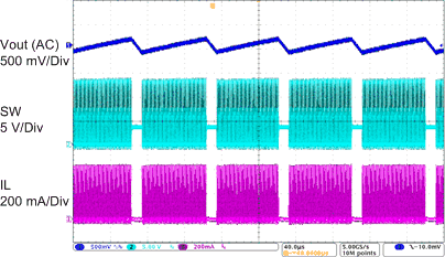
| Vin=3.6 V, Vout=12 V, Iout=30 mA | ||
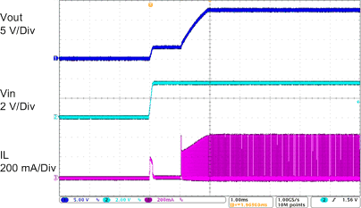
| Vin=3.6 V, Vout=12 V, Iout=25 mA | ||
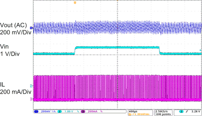
| Vin=3.0 V to 3.6 V, Vout=12 V, Iout=20 mA | ||
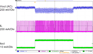
| Vin=3.6 V, Vout=12 V, Iout=5 mA to 20 mA | ||
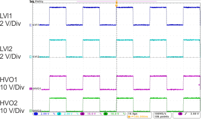
| LVI1 = LVI2 = 3.2 V, HVO1 = HVO2 = 12 V | ||
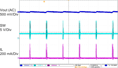
| Vin=3.6 V, Vout=12 V, Iout=2 mA | ||
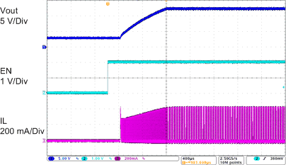
| Vin=3.6 V, Vout=12 V, Iout=25 mA | ||
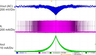
| Vin=3.6 V, Vout=12 V, Iout=0 mA to 30 mA | ||
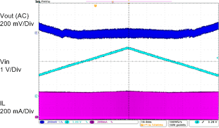
| Vin=1.8 V to 4.2 V, Vout=12 V, Iout=20 mA | ||